
User guide
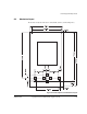

CLCD Display and Adaptor Board
ARM DUI 0224I Copyright © 2003-2010 ARM Limited. All rights reserved. C-15
C.4 Connectors
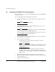
This section describes the connectors present on the CLCD adaptor board. For details
of the connectors present on the PB926EJ-S, see Appendix A Signal Descriptions.
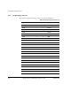
C.4.1 Interface connector
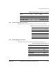
The signals on the CLCD interface connector J2 are shown in Table C-4.
Table C-4 CLCD interface connector J2
Pin Signal Pin Signal Pin Signal Pin Signal
1 B0 2 B2 35 B1 36 B3
3 B4 4 B6 37 B5 38 B7
5 G0 6 G2 39 G1 40 G3
7 G4 8 G6 41 G5 42 G7
9 R0 10 R2 43 R1 44 R3
11 R4 12 R6 45 R5 46 R7
13 CLLE 14 CLAC 47 GND 48 GND
15 CLCP 16 CLLP 49 GND 50 GND
17 CLFP 18 TSnKPADIRQ 51 GND 52 GND
19 TSnPENIRQ 20 TSnDAV 53 GND 54 LCDID0
21 TSSCLK 22 TSnSS 55 LCDID1 56 LCDID2
23 TSMISO 24 TSMOSI 57 LCDID3 58 LCDID4
25 LCDXWR 26
LCDSD0 59 GND 60 GND
27 LCDXRD 28 LCDXCS 61 GND 62 3V3
29 LCDDATAnCOMM 30 LCDSD0DIR 63 3V3 64 5V
31 CLPOWER 32 nLCDIOON 65 5V 66 VIN
33 PWRFIXEDSWITCH 34 VDDPOSSWITCH 67 VIN 68 VDDNEGSWITCH