
User guide


Hardware Description
3-6 Copyright © 2003-2010 ARM Limited. All rights reserved. ARM DUI 0224I
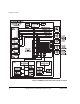
There are also two expansion master buses (AHB M1 and AHB M2) and
one expansion slave bus (AHB S). The expansion bus bridges are
configurable to support different performance and complexity trade-offs.
A bus matrix inside the ARM926EJ-S PXP Development Chip manages
the multiple paths between each master and the peripherals and memory.
The AHB Monitor provides information on bus accesses that can be
recorded by an attached logic analyzer. The bus accesses and other
performance information can be recorded to aid software profiling. See
AHB monitor on page 3-16 and the ARM926EJ-S PXP Development Chip
Reference Manual for more information.
Memory controllers
The ARM926EJ-S PXP Development Chip includes a multi-port
memory controller (for dynamic memory) and a static memory
controller. Both controllers have 32-bit interfaces to external memory.
See Memory interface on page 3-15.
DMA controller
The PrimeCell DMAC enables peripheral-to-memory,
memory-to-peripheral, peripheral-to-peripheral, and
memory-to-memory transactions. See DMA on page 3-65.
Interrupt controller
The PrimeCell VIC provides an interface to the interrupt system and
provides vectored interrupt support for high-priority interrupt sources
from:
• peripherals in the ARM926EJ-S PXP Development Chip
• peripherals in the FPGA (a secondary interrupt controller is present
in the FPGA)
• peripherals in expansion Logic Tiles.
See Interrupts on page 3-72.
CLCD controller
The CLCDC provides a flexible display interface that supports a VGA
monitor and color or monochrome LCD displays. See CLCDC interface
on page 3-61.
UARTs The UARTs perform serial-to-parallel conversion on data received from
a peripheral device and parallel-to-serial conversion on data transmitted
to the peripheral device. See UART interface on page 3-88.