
User guide

Hardware Description
ARM DUI 0224I Copyright © 2003-2010 ARM Limited. All rights reserved. 3-11
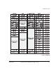
External masters drive the ARM926EJ-S PXP Development Chip AHB S port which
goes through an AHB-AHB bridge to the expansion master port on the matrix. This
master can access most of the slaves within the ARM926EJ-S PXP Development Chip,
including the GX175 MPMC (SDRAM controller), the PL093 SSMC (static memory
controller), and the expansion slaves.
External slaves are connected to the ARM926EJ-S PXP Development Chip AHB M1
and AHB M2 ports. Two of the expansion slave ports on the internal bus matrix are fed
to AHB-AHB bridges which drive the AHB M1 and AHB M2 ports. These ports are
accessible by all five of the internal masters and the expansion master connected to the
AHB S port.
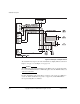
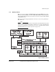
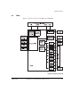
Simultaneous access
Figure 3-3 on page 3-12 shows how the matrix allows multiple masters to use the buses
at the same time:
• The ARM926EJ-S Data AHB master is accessing
0x10004000
and this decodes to
the external AHB M2 bus (the CODEC interface in the FPGA).
• The ARM926EJ-S Instruction AHB master is accessing
0x02000000
and this
decodes to dynamic memory on one of the MPMC slaves (DYCS0).
• The CLCDC master is accessing
0x01000000
and this decodes to dynamic memory
on one of the MPMC slaves (DYN CS0). The MPMC will manage the multiple
accesses to the slave ports.
• The DMAC is doing a memory to peripheral transfer. DMA master 1 is accessing
0x38000000
which decodes to static memory (SRAM). DMA master 0 is accessing
0x80000000
which is mapped to the AHB M1 bus (if a Logic Tile is installed, the
tile must decode this access and provide a response).
• An external master in the PCI controller or a Logic Tile is accessing
0x101F0000
and this decodes to the DMA APB.