R P/I-XP6NP5 Pentium Pro Motherboard USER'S MANUAL
USER'S NOTICE No part of this product, including the product and software may be reproduced, transmitted, transcribed, stored in a retrieval system, or translated into any language in any form by any means without the express written permission of ASUSTeK COMPUTER INC. (hereinafter referred to as ASUS) except documentation kept by the purchaser for backup purposes.
ASUS CONTACT INFORMATION ASUSTeK COMPUTER INC. Marketing Info: Address: 150 Li-Te Road, Peitou, Taipei, Taiwan, ROC Telephone: 886-2-894-3447 Fax: 886-2-894-3449 Email: info@asus.com.tw Technical Support: Fax: BBS: Email: WWW: Gopher: FTP: 886-2-895-9254 886-2-896-4667 tsd@asus.com.tw http://www.asus.com.tw/ gopher.asus.com.tw ftp.asus.com.
CONTENTS I. INTRODUCTION ........................................................ 1 How this manual is organized .......................................................... 1 Item Checklist .................................................................................. 1 II. FEATURES ................................................................. 2 Features of the ASUS Motherboard ................................................. 2 Parts of the ASUS Motherboard .........................................
CONTENTS Details of Power Management Setup ................................. 40 PNP and PCI Setup .................................................................. 42 Details of PNP and PCI Setup ............................................ 42 Load BIOS Defaults ................................................................. 44 Load Setup Defaults ................................................................. 44 Supervisor Password and User Password ................................
FCC & DOC COMPLIANCE Federal Communications Commission Statement This device complies with FCC Rules Part 15. Operation is subject to the following two conditions: • • This device may not cause harmful interference, and This device must accept any interference received, including interference that may cause undesired operation. This equipment has been tested and found to comply with the limits for a Class B digital device, pursuant to Part 15 of the FCC Rules.
I. INTRODUCTION I. INTRODUCTION (Manual / Checklist) How this manual is organized This manual is divided into the following sections: I. Introduction: Manual information and checklist II. Features: Information and specifications concerning this product III. Installation: Instructions on setting up the motherboard. IV. BIOS Setup: BIOS software setup information. V. DMI Utility: BIOS supported Desktop Management Interface VI. ASUS PCI-SC200: Installation of an optional Fast SCSI card. VII.
II. FEATURES Features of the ASUS Motherboard The ASUS P/I-XP6NP5 is carefully designed for the demanding PC user who wants a great many features in a small package. This motherboard: II. FEATURES (Features) 2 • Easy Installation: Is equipped with BIOS that supports auto detection of hard drives, PS/2 mouse, and Plug and Play devices to make setup of hard drives, expansion cards, and other devices virtually automatic. • Multi-Speed Support: Supports one 150-200MHz Pentium Pro CPU on a ZIF Socket 8.
• PCI Bus Master IDE Controller: Comes with an onboard PCI Bus Master IDE controller with two connectors that supports four IDE devices in two channels, provides faster data transfer rates, and supports Enhanced IDE devices such as Tape Backup and CD-ROM drives. This controller supports PIO Modes 3 and 4 and Bus Master IDE DMA Mode 2. BIOS now supports IDE CDROM or SCSI bootup. • Optional IrDA Connector: This motherboard supports an optional infrared port module for wireless interface.
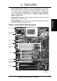
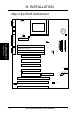
III. INSTALLATION CPU ZIF Socket 8 COM 1 JP1 JP2 JP3 JP4 Map of the ASUS Motherboard #CR2032 3Volt Button Cell Battery PS/2 Keyboard PS/2 Mouse CPU Voltage ID JP7 JP6 Parallel Printer Battery Test Lead 12V Fan Power Reg/ATX 3.3V Board Power Input for ATX Power Supply JP8 JP9 SIMM Socket 3 (Bank 1) SIMM Socket 2 (Bank 0) JP10 JP11 JP12 JP13 SIMM Socket 1 (Bank 0) Primary IDE COM 2 SIMM Socket 4 (Bank 1) Secondary IDE III. INSTALLATION (Map of Board) Floppy Drives BUS Freq. Freq.
III. INSTALLATION Jumpers 1) 2) 3) 4) 5) 6) 7) 8) JP14 JP17 JP16 JP7 JP8, JP9 JP10, 11, 12, 13 JP1, 2, 3, 4 JP6 p. 7 p. 7 p. 8 p. 9 p. 10 p. 10 p. 11 p. 11 Multi-I/O Selection (Enable/Disable) Flash ROM Boot Block Program (Enable/Disable) Real Time Clock RAM (Operation/Clear Data) Battery Test Lead (Operation/Test Mode) CPU External Clock (BUS) Frequency Selection CPU:BUS Frequency Ratio Selection Voltage ID 3, 2, 1, 0 for CPU (2.1V to 3.5V) 3.3Volt Power Source (Regulator/ATX Supply) p. 12 p. 15 p.
III. INSTALLATION Installation Steps Before using your computer, you must complete the following six steps: 1. 2. 3. 4. 5. 6. Set Jumpers on the Motherboard Install DRAM (and SRAM) Memory Modules Install the Central Processing Unit (CPU) Install Expansion Cards Connect Ribbon Cables, Cabinet Wires, and Power Supply Setup the BIOS Software 1. Jumpers III. INSTALLATION (Jumpers) Several hardware settings are made through the use of jumper caps to connect jumper pins (JP) on the motherboard.
III. INSTALLATION 1. Onboard Multi-I/O Selection (JP14) You can disable the onboard Multi-I/O (floppy, serial, parallel, and IrDA) through BIOS (see CHIPSET FEATURES SETUP) and with the following jumper in order to use your own Multi-I/O card. JP14 [1-2] (Default) [2-3] JP14 1 2 3 Enable I/O (Default) JP14 1 2 3 Disable I/O III. INSTALLATION (Jumpers) Multi-I/O Enable Disable Super Multi-I/O (Enable / Disable) 2.
III. INSTALLATION 3. Real Time Clock (RTC) RAM (JP16) This clears the user-entered information stored in the CMOS RAM of the Real Time Clock such as hard disk information and passwords. To clear the RTC data: (1) Turn off the PC, (2) Short this jumper, (3) Power on the PC, (4) Turn off the PC, (5) Remove this jumper, (6) Power on the PC, (7) Hold down during bootup and enter BIOS setup to re-enter user preferences. RTC RAM Operation Clear Data JP16 [2-3] (Default) [1-2] (momentarily) III.
III. INSTALLATION JP7 JP7 Operation Test Mode III. INSTALLATION (Jumpers) 4. Battery Test Lead (JP7) The Real Time Clock RAM is powered by the onboard button cell battery. You can test the battery’s current by removing this jumper and attaching a current meter to each pin. WARNING: You must unplug the power cord to your power supply to ensure that there is no power to your motherboard. The RTC RAM containing BIOS setup information will be cleared by this action.
III. INSTALLATION 5. CPU External Clock (BUS) Frequency Selection (JP8, JP9) These jumpers tells the clock generator what frequency to send to the CPU. These allow the selection of the CPU’s External frequency (or BUS Clock). The BUS Clock times the BUS Ratio equals the CPU's Internal frequency (the advertised CPU speed). 6.
III. INSTALLATION 7. Voltage Regulator Output Selection (JP1, 2, 3, 4) Pentium Pro Processors may require different voltages. Current processors (marked "Pentium Pro") support VID and will automatically adjust the voltage regulator so that no jumper settings are needed (leave these jumpers open in this case). Older processors without VID support require manual voltage ID setting. Use [S] for Short and [O] or Open. Voltage JP1 (VID 3) JP2 (VID 2) JP3 (VID 1) JP4 (VID 0) 3.5 [S] [S] [S] [S] 3.
III. INSTALLATION 2. System Memory (DRAM & SRAM) This motherboard supports four 72-pin SIMMs (Single Inline Memory Modules) of 4MB, 8MB, 16MB, 32MB, 64MB to form a memory size between 8MB to 256MB. The DRAM can be either 60ns or 70ns Fast Page Mode (Asymmetric or Symmetric), Extended Data Output (EDO), or Burst Extended Data Output (BEDO). SIMMs must be installed in pairs so that each bank contains two of the same size memory modules.
III. INSTALLATION DRAM Memory Installation Procedures: 1. The SIMM memory modules will only fit in one orientation as shown because of a "Plastic Safety Tab" on one end of the SIMM sockets which requires the "Notched End" of the SIMM memory modules. III. INSTALLATION (DRAM Memory) 1 2 3 4 Notched End 72 Pin SIMM DRAM Sockets & Module 2. Press the memory module firmly into place starting from a 45 degree angle making sure that all the contacts are aligned with the socket. 3.
III.
III. INSTALLATION 3. Central Processing Unit (CPU) The motherboard provides a 387-pin ZIF Socket 8. The CPU that came with the motherboard should have a fan attached to it to prevent overheating. If this is not the case then purchase a fan before you turn on your system. Apply thermal jelly to the CPU top and then install the fan onto the CPU. WARNING: Without a fan, the CPU can overheat and cause damage to both the CPU and the motherboard. (See "CPU Cooling Fan Connector" in this section). III.
III. INSTALLATION 4. Expansion Cards First read your expansion card documentation on any hardware and software settings that may be required to setup your specific card. NOTE: PCI Slot 5 has a MediaBus extension 2.0 (see page 18) which allows the installation of a PCI card or a MediaBus card (optional multifunctional card) but not both. WARNING: Make sure that you unplug your power supply when adding or removing expansion cards or other system components.
III. INSTALLATION Both ISA and PCI expansion cards may need to use IRQs. System IRQs are available to cards installed in the ISA expansion bus first, and any remaining IRQs are then used by PCI cards. Currently, there are two types of ISA cards. The original ISA expansion card design, now referred to as “Legacy” ISA cards, requires that you configure the card’s jumpers manually and then install it in any available slot on the ISA bus. You may use Microsoft's Diagnostic (MSD.
(This page was intentionally left blank) 18 ASUS P/I-XP6NP5 User’s Manual
III. INSTALLATION 5. External Connectors WARNING: Some pins are used for connectors or power sources. These are clearly separated from jumpers in "Map of the Motherboard" on page 4. Placing jumper caps over these will cause damage to your motherboard. IMPORTANT: Ribbon cables should always be connected with the red stripe on the Pin 1 side of the connector. The four corners of the connectors are labeled on the motherboard. Pin 1 is the side closest to the power connector on hard drives and floppy drives.
III. INSTALLATION 5. ATX Power Connector (20-pin block) This connector connects to a ATX power supply. The plug from the power supply will only insert in one orientation because of the different hole sizes. Find the proper orientation and push down firmly making sure that the pins are aligned. CAUTION: To prevent electrical spikes, make sure that the power supply is not connected to an outlet when making or removing connections. Power supplies contain power reserves which can damage electrical components.
III. INSTALLATION 7. Primary / Secondary IDE connectors (Two 40-pin Block) These connectors support the provided IDE hard disk ribbon cable. After connecting the single end to the board, connect the two plugs at the other end to your hard disk(s). If you install two hard disks, you must configure the second drive to Slave mode by setting its jumper accordingly. Please refer to the documentation of your hard disk for the jumper settings.
III. INSTALLATION 9. System Power LED (TB LED) This 2-pin connector lights the system power LED when the motherboard has power. Works the same as the next System Power LED. See the figure on the next page. III. INSTALLATION (Connectors) 10. SMI Suspend Switch Lead (SMI) This allows the user to manually place the system into a suspend mode or "Green" mode where system activity will be instantly decreased to save electricity and expand the life of certain components when the system is not in use.
III. INSTALLATION 14. Speaker Connector (SPEAKER) This 4-pin connector connects to the case-mounted speaker. System Power LED SMI Lead ATX Power Switch Reset SW +5V GND GND +5V NC GND LOCK GND +5V GND GND GND SPKR System Power LED Keyboard Lock Speaker Connector III.
III. INSTALLATION 15. CPU Cooling Fan Connector (FAN) This connector supports a CPU cooling fan of 500mAMP (6WATT) or less. Orientate the fan so that the heat sink fins allow airflow to go across the onboard heat sink(s) instead of the expansion slots. Depending on the fan manufacturer, the wiring and plug may be different. The red wire should be positive, while the black should be ground. Connect the fan's plug to the board taking into consideration the polarity of the this connector.
III. INSTALLATION Power Connection Procedures III. INSTALLATION (Power Connections) 1. After all jumpers and connections are made, close the system case cover. 2. Make sure that all switches are in the off position as marked by . 3. Connect the power supply cord into the power supply located on the back of your system case as instructed by your system user's manual. 4. Connect the power cord into an power outlet that is equipped by a surge protector. 5.
IV. BIOS SOFTWARE Support Software FILELIST.TXT - View this file to see the files included in the support software. PFLASH.EXE - This is the Flash Memory Writer utility that updates the BIOS by uploading a new BIOS file to the programmable flash ROM chip on the motherboard. To determine the BIOS version, check the last four numbers of the code displayed on the upper left-hand corner of your screen during bootup. Larger numbers represent a newer BIOS file.
IV. BIOS SOFTWARE 2. Update BIOS Main Block from File This option updates the BIOS from a file on the disk. This can either be a new file or a backup file created by the “Save Current BIOS to File” option. This will not update the Boot Block if the Boot Block is different. You will be prompted with the following if advanced features if necessary. Boot Block of New BIOS is different from old one !!! Please Use 'Advanced Feature' to flash whole bios !!! 3.
IV. BIOS SOFTWARE Updating your Motherboard's BIOS 1. Download an updated BIOS file from a Bulletin Board Service (BBS) or the internet (WWW) and save to the diskette you created in step 1 of the Main Menu. Visit ASUS WWW at http://www.asus.com.tw/ or FTP: ftp.asus.com.tw/ pub/ASUS or see ASUS CONTACT INFORMATION on page II. 2. Turn off your computer and open the system cabinet to Enable "Boot Block Programming" jumper as shown in section III. 3.
IV. BIOS SOFTWARE 6. BIOS Setup The motherboard supports two programmable Flash ROM chips: 5 Volt and 12 Volt. Either of these memory chips can be updated when BIOS upgrades are released. Use the Flash Memory Writer utility to download the new BIOS file into the ROM chip as described in detail in this section. All computer motherboards provide a Setup utility program for specifying the system configuration and settings.
IV. BIOS SOFTWARE Load Defaults The “Load BIOS Defaults” option loads the minimized settings for troubleshooting. “Load Setup Defaults”, on the other hand, is for loading optimized defaults for regular use. Choosing defaults at this level, will modify all applicable settings. A section at the bottom of the above screen displays the control keys for this screen. Take note of these keys and their respective uses.
IV. BIOS SOFTWARE Details of Standard CMOS Setup: Date To set the date, highlight the “Date” field and then press the page up/page down or +/- keys to set the current date. Follow the month, day and year format. Valid values for month, day and year are: Month: Day: Year: 1 to 12 1 to 31 up to 2099 Time To set the time, highlight the “Time” field and then press the page up/page down or +/- keys to set the current time. Follow the hour, minute and second format.
IV. BIOS SOFTWARE For IDE hard disk drive setup, you can: • Use the Auto setting for detection during bootup. • Use the IDE HDD AUTO DETECTION in the main menu to automatically enter the drive specifications. • Enter the specifications yourself manually by using the “User” option. The entries for specifying the hard disk type include CYLS (number of cylinders), HEAD (number of read/write heads), PRECOMP (write precompensation), LANDZ (landing zone), SECTOR (number of sectors) and MODE.
IV. BIOS SOFTWARE Drive A / Drive B (None) These fields record the types of floppy disk drives installed in your system. The available options for drives A and B are: 360KB, 5.25 in.; 1.2MB, 5.25 in.; 720KB, 3.5 in.; 1.44MB, 3.5 in.; 2.88MB, 3.5 in.; None To enter the configuration value for a particular drive, highlight its corresponding field and then select the drive type using the left- or right-arrow key. Floppy 3 Mode Support (Disabled) This is the Japanese standard floppy drive.
IV. BIOS SOFTWARE BIOS Features Setup This “BIOS Features Setup” option consists of configuration entries that allow you to improve your system performance, or let you set up some system features according to your preference. Some entries here are required by the motherboard’s design to remain in their default settings. A section at the lower right of the screen displays the control keys you can use. Take note of these keys and their respective uses.
IV. BIOS SOFTWARE CPU Fast String (Enabled) Leave on default setting of Enabled for best performance. Deturbo Mode (Disabled) When Enabled, FLUSH# signal is held asserted to disable caching and the P6 bus pipeline will be stalled. This allows software to run at a reduced-speed. The default is set to Disabled to allow maximum processing speed. Quick Power On Self Test (Enabled) This field speeds up the Power-On Self Test (POST) routine by skipping retesting a second, third, and forth time.
IV. BIOS SOFTWARE Typematic Rate Setting (Disabled) When enabled, you can set the two typematic controls listed next. Setup default setting is Disabled. Typematic Rate (Chars/Sec) This field controls the speed at which the system registers repeated keystrokes. Options range from 6 to 30 characters per second. Setup default setting is 6; other settings are 8, 10, 12, 15, 20, 24, and 30. Typematic Delay (Msec) (250ms) This field sets the time interval for displaying the first and second characters.
IV. BIOS SOFTWARE Chipset Features Setup (BIOS Features) This “Chipset Features Setup” option controls the configuration of the board’s chipset. Control keys for this screen are the same as for the previous screen. NOTE: SETUP Defaults are noted in parenthesis next to each function heading. Details of Chipset Features Setup ASUS P/I-XP6NP5 User's Manual IV. BIOS (Chipset Features) Auto Configuration The default setting of 60ns DRAM sets the optimal timings for items 2 through 6 for 60ns DRAM modules.
IV. BIOS SOFTWARE (Chipset Features) Read-Around-Write The default setting of Enabled will increase the execution efficiency of the processor. It allows the processor to execute read commands out of order if there is no dependence between these read and other write commands.
IV. BIOS SOFTWARE Onboard FDC Swap A: B: (No Swap) This field reverses the drive letter assignments of your floppy disk drives. Two options are available: “No Swap” and “Swap AB.” If you want to switch drive letter assignments, set this field to “Swap AB”, and the swap will be controlled in hardware. This works separately from the BIOS Features floppy disk swap feature. It is functionally the same as physically interchanging the connectors of the floppy disk drives.
IV. BIOS SOFTWARE Power Management Setup This “Power Management Setup” option allows you to reduce power consumption. This feature turns off the video display and shuts down the hard disk after a period of inactivity. IV. BIOS (Chipset Features) NOTE: SETUP Defaults are noted in parenthesis next to each function heading. Details of Power Management Setup IV. BIOS (Power Management) Power Management (User Defined) This field acts as the master control for the power management modes.
IV. BIOS SOFTWARE Video Off Method (V/H SYNC + Blank) This field defines the video off features. Three options are available: V/H SYNC + Blank, DPMS, and Blank Only. The first option, which is the default setting, blanks the screen and turns off vertical and horizontal scanning; DPMS (Display Power Management System) allows the BIOS to control the video display card if it supports the DPMS feature; Blank Screen only blanks the screen.
IV. BIOS SOFTWARE PNP and PCI Setup This “PNP and PCI Setup” option configures the PCI bus slots. All PCI bus slots on the system use INTA#, thus all installed PCI cards must be set to this value. NOTE: SETUP Defaults are noted in parenthesis next to each function heading. Details of PNP and PCI Setup IV. BIOS (Plug & Play / PCI) The first four fields on the screen set how IRQ use is determined for each PCI slot. The default setting for each field is Auto, which uses auto-routing to determine IRQ use.
IV. BIOS SOFTWARE DMA x Used By ISA (No/ICU) These fields indicate whether or not the displayed DMA channel for each field is being used by a Legacy (non-PnP) ISA card. Available options include: No/ICU and Yes. The first option, the default setting, indicates either that the displayed DMA channel is not used or an ICU is being used to determine if an ISA card is using that channel.
IV. BIOS SOFTWARE Load BIOS Defaults This “Load BIOS Defaults” option allows you to load the troubleshooting default values permanently stored in the BIOS ROM. These default settings are non-optimal and disable all high performance features. To load these default settings, highlight “Load BIOS Defaults” on the main screen and then press the key. The system displays a confirmation message on the screen. Press the key and then the key to confirm.
IV. BIOS SOFTWARE Supervisor Password and User Password IV. BIOS (Passwords) These two options set the system passwords. “Supervisor Password” sets a password that will be used to protect the system and the Setup utility; “User Password” sets a password that will be used exclusively on the system. By default, the system comes without any passwords. To specify a password, highlight the type you want and then press the key. A password prompt appears on the screen.
IV. BIOS SOFTWARE IDE HDD Auto Detection This “IDE HDD Auto Detection” option detects the parameters of an IDE hard disk drive, and automatically enters them into the Standard CMOS Setup screen. ROM PCI/ISA BIOS (PI-XP6NP5) CMOS SETUP UTILITY AWARD SOFTWARE, INC.
IV. BIOS SOFTWARE IMPORTANT: If your hard drive was already formatted on an older previous system, incorrect parameters may be detected. You will need to enter the correct parameters manually or use low-level format if you do not need the data stored on the hard drive. If the parameters listed differ from the ones used when the drive was formatted, the drive will not be readable. If the auto-detected parameters do not match the ones that should be used for your drive, do not accept them.
(This page was intentionally left blank) 48 ASUS P/I-XP6NP5 User's Manual
V. DESKTOP MANAGEMENT Desktop Management Interface (DMI) Introducing the ASUS DMI Configuration Utility System Requirements The motherboard BIOS must support DMI. The following motherboards do not support DMI: • P/I-P6RP4 • PCI/E-P54NP4 • PCI/I-P54NP4D (not supported) (not supported) (not supported) V. DMI (DMI Introduction) (Flash Memory Writer) This motherboard supports DMI within the BIOS level and provides a DMI Configuration Utility to maintain the Management Information Format Database (MIFD).
V. DESKTOP MANAGEMENT Using the ASUS DMI Configuration Utility Edit DMI (or delete) Use the ←→ (left-right) cursors to move the top menu items and the ↑↓ (up-down) cursor to move between the left hand menu items. The bottom of the screen will show the available keys for each screen. Press enter at the menu item to enter the right hand screen for editing. “Edit component” appears on top. The reversed color field is the current cursor position and the blue text are available for editing.
V. DESKTOP MANAGEMENT Save MIFD You can save the MIFD (normally only saved to flash ROM) to a file by entering the drive and path here. If you want to cancel save, you may press ESC and a message “Bad File Name” appears here to show it was not saved. Load MIFD You can load the disk file to memory by entering a drive and path and file name here. V. DMI (Using DMI Utility) Load BIOS Defaults You can load the BIOS defaults from a MIFD file and can clear all user modified and added data.
(This page was intentionally left blank) 52 ASUS P/I-XP6NP5 User's Manual
VI. ASUS PCI-SC200 SCSI Card VI. ASUS PCI-SC200 (NCR SCSI BIOS) NCR SCSI BIOS and Drivers Aside from the system BIOS, the Flash memory chip on the motherboard also contains the NCR SCSI BIOS. This SCSI BIOS works in conjunction with the optional ASUS PCI-SC200 SCSI controller card to provide a complete PCI Fast SCSI-2 interface. All SCSI devices you install to your system require driver software to function. The NCR SCSI BIOS directly supports SCSI hard disks under the DOS, Windows and OS/2 environments.
VI. ASUS PCI-SC200 SCSI Card VI. ASUS PCI-SC200 (Setup) The ASUS PCI-SC200 SCSI Interface Card Your motherboard may have come with an optional SCSI (Small Computer System Interface) controller card, the PCI-SC200. The card is also available separately. This card works with the SCSI BIOS on the motherboard. Together, they provide a complete PCI Fast SCSI-2 interface. With the card installed in your system you can connect SCSI devices installed in your system case to the internal connector on the card.
VI. ASUS PCI-SC200 SCSI Card VI. ASUS PCI-SC200 (Jumpers) Setting the INT Assignment You must use PCI INT A setting in order to properly assign the card's interrupt. On the ASUS PCI-SC200, you assign the INT by setting jumper JP1 or JP2. The default setting for the card already is INT A, so you do not need to change the setting to use the ASUS PCI-SC200 with this motherboard.
VI. ASUS PCI-SC200 SCSI Card VI. ASUS PCI-SC200 (SCSI ID Numbers) Decide whether or not you need to terminate the ASUS PCI-SC200 based on its position in the SCSI chain. Only the devices at each end of the chain need to be terminated. If you have only internal or only external devices connected to the ASUS PCI-SC200, then you must terminate the ASUS PCI-SC200. If you have both internal and external devices connected, you must not terminate the card. See the following example which illustrates this concept.
VII. ASUS I-A16C Audio Card NOTE: The ASUS I-A16C 16-bit ISA audio card comes with certain motherboard packages and is not for sale separately. ASUS I-A16C Audio Features Creative Labs ViBRA 16C PnP Audio Chip Full Duplex Supports 16/8 bit PCM 5KHz to 44.1KHz Wave Table Upgradeable Software Includes: DOS and Window 3.1 Drivers Windows 95 Driver Wave Editor Wave OLE Quick CD Mixer Control Quick Player VII.
VII. ASUS I-A16C Audio Card Layout and Connectors Mitsumi Audio In Sony Audio In Panasonic Audio In PC Speaker In Volume Control Wave Table Upgrade PC Speaker Out Speaker Out Line Out VII. ASUS I-A16C (Layout / Connectors) Line In Microphone MIDI/Game Connectors The audio input connectors are used when you wish to control software mixer settings (bass, treble, volume, etc.) for audio CD's that are played with your CD-ROM.