
User Manual


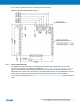
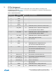
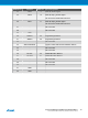
Table Of Contents

1. Integrated Devices and Block Diagram
1.1. Module Block Diagram
Figure 1-1 Module Block Diagram
ATSAMR21G18-MR210UA
AT45DB041E
ATECC508
4-Mbit DataFlash
CryptoAuthentication
Device
Balun &
Harmonic Filter
Antenna Diversity
Switch
U.Fl
50Ohm
U.Fl
50Ohm
1 GPIO
17 GPIO
SPI
SWI
ATSAMR21G18
ARM
®
Cortex
®
-M0+
1.2. Integrated Peripherals
1.2.1. Serial Flash Interconnection
Table 1-1 Serial Flash Interconnection
DataFlash Signal MCU Function MCU Pin Port and SERCOM Configuration
SO MISO 37 PA22 SERCOM5 PAD[2] DIPO=0x2
SI MOSI 38 PA23 SERCOM5 PAD[3] DOPO=0x2
SCK SCK 48 PB03 SERCOM5 PAD[1] DOPO=0x2
#CS GPIO 47 PB02 to be set low in software before SPI access
The signals in this table are not available as module I/O. More information about the FLASH IC can be
found in its related datasheet [ADESTO].
1.2.2. UART with Hardware Flow Control (RTS/CTS)
For an Application where the ADC is not in use, SERCOM0 can be multiplexed as shown in the table
below.
Table 1-2 UART with Hardware Flow Control (RTS/CTS)
Module Pin MCU Function MCU Pin Port and SERCOM Configuration
14 UART TX 15 SERCOM0; MUX=C; PAD[0] TXPO=0x2
25 UART RX 10 SERCOM0; MUX=D; PAD[1] RXPO=0x1
Atmel ATSAMR21G18-MR210UA [DATASHEET]
Atmel-42475B-ATSAMR21G18-MR210UA_Datasheet_Preliminary-09/2015
4