
User Manual


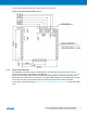
Table Of Contents

2. Mechanical Description
2.1. Mechanical Dimensions
Dimensions are in mm. The module pins are arranged with a 1mm pitch distance. The module is
designed in a symmetric way.
Figure 2-1 Module Bottom Dimensions ( Seen from a CAD top perspective )
The module can be mounted to a base board with a soldered RF connection. For this case one or both
U.Fl connectors are left unconnected and the RF pads on the bottom side are used to feed an antenna
located on the base board.
2.2. Footprint and Layout Recommendation
Since the module does not contain an antenna, the module does not set any limits for the base board
material selection or the board stack-up construction. The module does also not require a certain
positioning on the board in relation to the board edge. The module must be placed away from interference
sources on the base board like clock oscillators or step converters. The area underneath the module must
be filled with a grounded copper plane. The RF-Pad area needs special attention. The following sections
provide more information on that.
A typical design is supposed to connect the I/O ring to the base board while the antenna feeds are using
the U.Fl connectors. Using the antennas in Approved Antennas on page 16, the modular approval for
the final product can be used without re-certification.
2.2.1. Design without RF-Pads
For a design without U.Fl connected antennas, the base board design has to have no copper fill within the
RF-Pad area (*!). All layers with less than 0.5mm distance from top shall not be filled with copper
underneath the RF-Pad area.
Atmel ATSAMR21G18-MR210UA [DATASHEET]
Atmel-42475B-ATSAMR21G18-MR210UA_Datasheet_Preliminary-09/2015
7