
User Manual


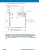
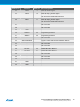
Table Of Contents

For all other I/O pads the geometry in below figure should be used.
Figure 2-2 Recommended Base Board Layout
2.2.2. Design without RF-Pads
For applications where the antenna is implemented on the base PCB, the RF-Pads can be used to
connect the RF signals. The pad layout is available in Figure 2-2 Recommended Base Board Layout on
page 8. The base board traces shall be designed with a line impedance of 50Ohm. Depending on the
base board stack construction a microstrip or a grounded coplanar design can be implemented. The best
choice will be the line type with the best match in between line width and the 0.8mm pad width.
For all other IO pads the geometry in Figure 2-2 Recommended Base Board Layout on page 8 should be
used.
Atmel ATSAMR21G18-MR210UA [DATASHEET]
Atmel-42475B-ATSAMR21G18-MR210UA_Datasheet_Preliminary-09/2015
8