
User's Manual
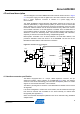
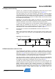
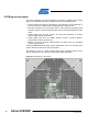
Table Of Contents

10
Atmel AVR2080
8479A-AVR-01/12
5 PCB layout description
This section describes critical layout details to be carefully considered during a PCB
design. The PCB design requires an optimal solution for the following topics:
• Create a solid ground plane for the antenna. The PCB has to be considered as a
part of the antenna; it interacts with the radiated electromagnetic wave
• Around the SE2431L front end module layout, ensure good RF grounding, good
thermal conduction, effective decoupling and correct microstrip impedances for RF
tracks
• Isolate digital noise from the antenna and the radio transceiver to achieve
optimum range and RF performance
• Isolate digital noise from the 16MHz reference crystal to achieve optimum
transmitter and receiver performance
• Reduce any kind of spurious emissions below the limits set by the individual
regulatory organizations
The Atmel REB231FE2 PCB design further demonstrates a low-cost, two-layer PCB
solution without the need of an inner ground plane.
The drawing in Figure 5-1 sho
ws critical sections using numbered captions. Each
caption number has its own subsection below with detailed information.
Figure 5-1. Board layout – RF section.