
User's Manual
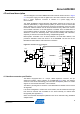
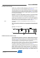
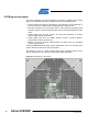
Table Of Contents

Atmel AVR2080
7
8479A-AVR-01/12
4.3 Supply current sensing
A jumper, JP1, is placed in the supply voltage trace to offer an easy way for current
sensing of active components one the Atmel REB231FE2, see Figure 4-4.
The po
wer supply pins of the radio transceiver and FEM are protected against
overvoltage stress and reverse polarity at the EXPAND1 pins (net CVTG, net DGND)
using a Zener diode (D1) and a thermal fuse (F1) (see appendix A.1). Thi
s is required
because the Atmel STK500 will provide 5V as default voltage, and the board can also
be mounted with reverse polarity.
Depending on the actual supply voltage, the diode D1 can consume several
milliamperes. This has to be considered when the current consumption of the whole
system is measured. In such a case, D1 should be removed from the board.
To achieve the best RF performance, the analog (EVDD, AGND) and digital (DEVDD,
DGND) supply are separated from each other by a CLC PI-element. Digital and
analog ground planes are connected together on the bottom layer, underneath the
radio transceiver IC. Further details are described in Chapter 5, pag
e 10.
NOTE All components connected to nets DEVDD/EVDD contribute to the total current
consumption.
While in radio transceiver SLEEP state, most of the supply current is drawn by the
1M pull-up resistor, R9, connected to the ID EEPROM and the EEPROM standby
current.
Figure 4-4. Power supply routing.
D1
BZG05C3V9
F1
MICROSMD035F
C30
100n
CVTG
DGND
C31
100n
L1
220Ohm@100MHz
JP1
X4
DEVDD EVDD
DGND
C18
4.7uF
C26
4.7uF
DGND
4.4 Radio transceiver reference clock
The integrated radio transceiver is clocked by a 16MHz reference crystal. The
2.4GHz modulated signal is derived from this clock. Operating the node according to
IEEE 802.15.4 [4], the ref
erence frequency must not exceed a deviation of ±40ppm.
The absolute frequency is mainly determined by the external load capacitance of the
crystal, which depends on the crystal type and is given in its datasheet.
The radio transceiver reference crystal, Q1, shall be isolated from fast switching
digital signals and surrounded by a grounded guard trace to minimize disturbances of
the oscillation. Detailed layout considerations can be found in Section 5.2.
The
REB uses a Siward CX4025 crystal with load capacitors of 10pF and 12pF. The
imbalance between the load capacitors was chosen to be as close as possible to the
desired resonance frequency with standard components. To compensate for
fabrication and environment variations, the frequency can be further tuned using the
radio transceiver register XOSC_CTRL (0x12) (refer to [1]). The
REB production test
guarantees a tolerance of within +20ppm and -5ppm. The correction value, to be