
User`s guide


Using the AT85DVK-07 Board
2-12 AT85DVK-07 Development Board User Guide
4391B–MP3–07/07
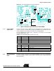
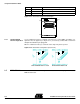
2.5 USB Unit
The USB unit provides all the required hardware to develop USB V2.0 full-speed and
high-speed devices and full-speed reduced-host / OTG compliant applications. It con-
sists in a USB mini AB connector (including ID pin) and an OTG extension connector
J24 (see Table 2-10) which allows control of an external VBUS power supply able to
power USB device.
Details on how to connect a USB storage device to the AT85DVK-07 Board are pro-
vided in Section 2.15.
Figure 2-10. USB Unit Implementation
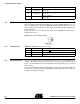
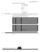
2.5.1 OTG Extension Table 2-10. OTG Extension Connector (J24)
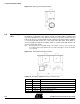
2.6 Nand Flash Unit
The Nand Flash unit consists in a standard nand flash memory foot print allowing user to
solder its own nand flash memory and 2 extension connectors J13 & J14 allowing inser-
tion of a 2x NF daughter board or a 4x NF daughter board supporting up to 2 or 4 nand
flash memories.
A 4x nand flash daughter board equipped with 1 memory along with a bare PCB (see
Section 2.16) is delivered inside the AT85DVK-07 Starter Kit. Figure 2-12 shows the
daughter-board plug-in orientation.
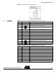
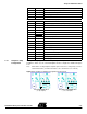
24 P0.4/SD4/LD4
PSI Slave Data Bit 4
LCD Data Bit 4
25 P0.7/SD7/LD7
PSI Slave Data Bit 7
LCD Data Bit 7
26 P0.6/SD6/LD6
PSI Slave Data Bit 6
LCD Data Bit 6
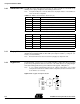
Pin Number Pin Name Pin Description
J25
J24
OTG
Pin Number Pin Name Pin Description
1 UVCON External VBUS ON/OFF control line
2 VBUS +5V VBUS from external power supply
3 VSS 0V digital supply reference