
Datasheet


49
AT89C5132
4173C–USB–07/04
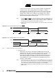
Figure 26. Timer 0 and Timer 1 Clock Controller and Symbols
Timer 0 Timer 0 functions as either a Timer or event Counter in four modes of operation.
Figure 27 through Figure 33 show the logical configuration of each mode.
Timer 0 is controlled by the four lower Bits of TMOD register (see Table 42) and Bits 0,
1, 4 and 5 of TCON register (see Table 41). TMOD register selects the method of Timer
gating (GATE0), Timer or Counter operation (C/T0#) and mode of operation (M10 and
M00). TCON register provides Timer 0 control functions: overflow flag (TF0), run control
bit (TR0), interrupt flag (IE0) and interrupt type control bit (IT0).
For normal Timer operation (GATE0 = 0), setting TR0 allows TL0 to be incremented by
the selected input. Setting GATE0 and TR0 allows external pin INT0# to control Timer
operation.
Timer 0 overflow (count rolls over from all 1s to all 0s) sets TF0 flag generating an inter-
rupt request.
It is important to stop Timer/Counter before changing mode.
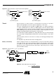
Mode 0 (13-bit Timer) Mode 0 configures Timer 0 as a 13-bit Timer which is set up as an 8-bit Timer (TH0 reg-
ister) with a modulo 32 prescaler implemented with the lower five Bits of TL0 register
(see Figure 27). The upper three Bits of TL0 register are indeterminate and should be
ignored. Prescaler overflow increments TH0 register. Figure 28 gives the overflow
period calculation formula.
Figure 27. Timer/Counter x (x = 0 or 1) in Mode 0
Figure 28. Mode 0 Overflow Period Formula
PER
CLOCK
TIM0
CLOCK
OSC
CLOCK
0
1
T0X2
CKCON.1
÷ 2
Timer 0 Clock
Timer 0 Clock Symbol
PER
CLOCK
TIM1
CLOCK
OSC
CLOCK
0
1
T1X2
CKCON.2
÷ 2
Timer 1 Cloc
k
Timer 1 Clock Symbol
TIMx
CLOCK
TRx
TCON Reg
TFx
TCON Reg
0
1
GATEx
TMOD Reg
÷ 6
Overflow
Timer x
Interrupt
Request
C/Tx#
TMOD Reg
THx
(8 Bits)
TLx
(5 Bits)
INTx
Tx
6 ⋅ (16384 – (THx, TLx))
TFx
PER
=
F
TIMx