ATAVRAUTO100 ..............................................................................................
Section 1 Introduction ........................................................................................... 1-4 1.1 Overview ...................................................................................................1-4 Section 2 Using the ATAVRAUTO100.................................................................. 2-6 2.1 2.2 2.3 2.4 2.5 2.6 Overview ...................................................................................................2-6 Power Supply ......................
Section 1 Introduction Congratulations on your selection of the ATAVRAUTO100. This board includes all elements necessary for designers to quickly develop code related to CAN and LIN communication gateway implementing the AT90CAN128 and for prototyping and testing of new designs. 1.1 Overview This document describes the ATAVRAUTO100, a board providing CAN and LIN networking resources.
Introduction 1.2 ATAVRAUTO100 Features The ATAVRAUTO100 provides the following features: AT90CAN128 QFN64, AVR Studio software interface (Note:), Power supply: – regulated 5.0V out of the VBAT (typical 12V) from the LIN connector JTAG connector: – for on-chip In Situ Programming (ISP) – for on-chip debugging using JTAG ICE Serial interfaces: – 1 CAN interface (High Speed and Low Speed) – 1 LIN interface 1.3 and 2.0 compliant (Software library available on the Atmel website for LIN 1.3).
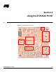
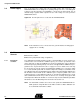
Section 2 Using the ATAVRAUTO100 2.1 Overview Figure 2-1.
Using the ATAVRAUTO100 2.2 Power Supply Th e on- board power supply mus t be pr ovi ded v ia the L IN connec tor. T he ATAVRAUTO100 has been designed for operating voltage from 7V to +18V with typical voltage at 12V. The LIN transceiver ATA6621, connected to the LIN network, has an internal voltage regulator which outputs 5.0V ±3%. This voltage is used to power the AT90CAN128 device. Figure 2-2. The LIN power line is used to bias the ATAVRAUTO100 Note: 2.
Using the ATAVRAUTO100 2.3.2 External crystal Necessary for the CAN network precision, the following crystal frequency allows proper ATAVRAUTO100 operations(1): 8MHz, 12MHz, 16MHz. The ATAVRAUTO100 comes with a default 8MHz crystal oscillator (CAN baut rate up to 1MBit/sec). The LIN master mode clock should always be a crystal or external clock oscillator. Currently, only 8MHz and 16MHz crystal oscillator is supported. Figure 2-3. Crystal Oscillator connection. Note: 2.4 On-board ressources 2.4.
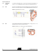
Using the ATAVRAUTO100 2.4.2 LIN MASTER selection To operate the LIN in Master mode, one 1kΩ resistor must be placed at the Master connection. To do so, the MSTR jumper must be positionned as indicated in Figure 2-4. 2.4.3 CAN Connection to the CAN network is made via the CAN connector JP2. Only the CAN- and CAN+ are connected. The signals are routed to ATA6660 CAN high speed transceiver. Figure 2-5. CAN High Speed connections 2.4.
Using the ATAVRAUTO100 2.5 In-System Programming The AT90CAN128 can be programmed using specific SPI links. This sub section will explain how to connect the programmer. The FLASH, EEPROM memory (and all Fuse and Lock Bit Option ISP-programmable) can be programmed individually or with the sequential automatic programming option. When programming, the NISP jumper has to be removed. Note: 2.5.
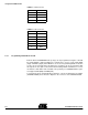
Using the ATAVRAUTO100 Table 2-1. ICE Connector PIN Function 7 VCC 8 NC 9 TDI 10 GND Table 2-2. ISP Connector 2.5.2 PIN Function 1 MISO 2 VCC 3 SCK 4 MOSI 5 NRES 6 GND Programming with AVR ISP via SPI Both the Flash and EEPROM memory arrays can be programmed using the serial SPI bus while RESET is pulled to GND. The serial interface consists of pins SCK, MOSI (input) and MISO (output).
Using the ATAVRAUTO100 Figure 2-8. Programming the ATAVRAUTO100 using ATAVRAUTO900 AVR ISP 2.5.3 Programming with AVR JTAGICE mkII The AT90CAN128can be preogrammed using specific JTAG link: 3-wire debug-wire interface. To use the AVR JTAGICE mkII with an ATAVRAUTO100 an optional adaptor should be used. Then the JTAG probe can be connected to the ATAVRAUTO100 as shown in the following figure. Figure 2-9. JTAGICEmkII probe connecting through debugWIRE interface.
Using the ATAVRAUTO100 2.6 Debugging 2.6.1 Debugging with AVR JTAGICEmkII The JTAGEN fuse must be programmed to enable the JTAG Test Access Port. In addition, the OCDEN fuse must be programmed and no Lock bits must be set for the Onchip debug system to work. As a security feature, the On-chip debug system is disabled when either of the LB1 or LB2 Lock bits are set. Otherwise, the On-chip debug system would have provided a back-door into a secured device.
Section 3 Technical Specifications System Unit – Physical Dimensions...............................................L=45 x W=45 x H=8 mm – Weight ........................................................................................................17 g Operating Conditions – Internal Voltage Supply ..... ...................................................................... 5.0V – External Voltage Supply .....................................................................
Section 4 Technical Support For Technical support, please contact avr@atmel.com. When requesting technical support, please include the following information: Which target AVR device is used (complete part number) Target voltage and speed Clock source and fuse setting of the AVR Programming method (ISP, JTAG or specific Boot-Loader) Hardware revisions of the AVR tools, found on the PCB Version number of AVR Studio. This can be found in the AVR Studio help menu.
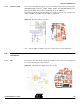
Section 5 Complete Schematics On the next pages, the following documents of ATAVRAUTO100 are shown: Complete schematics, Bill of materials Assembly drawing ATAVRAUTO100 User Guide 5-19 7697B–AUTO–09/07
Complete Schematics Figure 5-1.
Complete Schematics Figure 5-2.
Complete Schematics R9 C1 C7 Q1 R10 C3 D_WD MAST D3 D2 C2 R12 R13 U2 R11 C11 ICE&ISP D1R2 R1 DG C10 C8 C9 Y1 R5 NWAKE ATAVRAUTO100 User Guide CAN TERM1 CAN to LIN Gateway R3 C6 R4 TERM2 R6 R8 NISP BOOT C4 C5 U1 NRES ATAVRAUTO100 PM-06 V1.0 U3 R7 DB LIN Figure 5-3.
Atmel Corporation 2325 Orchard Parkway San Jose, CA 95131, USA Tel: 1(408) 441-0311 Fax: 1(408) 487-2600 Regional Headquarters Europe Atmel Sarl Route des Arsenaux 41 Case Postale 80 CH-1705 Fribourg Switzerland Tel: (41) 26-426-5555 Fax: (41) 26-426-5500 Asia Room 1219 Chinachem Golden Plaza 77 Mody Road Tsimshatsui East Kowloon Hong Kong Tel: (852) 2721-9778 Fax: (852) 2722-1369 Japan 9F, Tonetsu Shinkawa Bldg.