ATAVRAUTO200 ..............................................................................................
Table of Contents Section 1 Introduction ........................................................................................... 1-1 1.1 Overview ...................................................................................................1-1 Section 2 Using the ATAVRAUTO200.................................................................. 2-3 2.1 2.2 2.3 2.4 2.5 2.6 Overview ...................................................................................................2-3 Power Supply ...
Section 1 Introduction Congratulations on your purchase of the ATAVRAUTO200 board. This board includes all elements necessary for designers to quickly develop code related to LIN communication node implementing the ATmega88 and for prototyping and testing of new designs. 1.1 Overview This document describes the ATAVRAUTO200 dedicated to the ATmega88 AVR micro controllers. This board is designed to allow an easy evaluation of the product using demonstration firmware.
Introduction 1.2 ATAVRAUTO200 features The ATAVRAUTO200 provides the following features: ATmega88 QFN32 AVR Studio® software interface(1), Power supply – Regulated 5V – From LIN connector (LIN network power supply) JTAG connector: – for on-chip In Situ Programming (ISP) – for on-chip debugging using JTAG ICE DC Motor connector – DC Motor power supply output – Hall effect sensor(s) power supply and input(s) Serial interface: – 1 LIN interface 1.3 and 2.
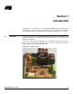
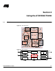
Section 2 Using the ATAVRAUTO200 2.1 Overview Figure 2-1. Board Overview U1LIN D1 Transceiver C2 Regulator NI P NISP C3 Connector R1 R2 R5 F1 LIN LI LIN C1 R14 R1 4 U2 Motor Motor Relay Connector ATmega88 R21 R2 Q2 HALL HA R19 R1 9 R22 C8R8R7 R13 R12 R1 2 R1 R10 R1 0 Current 3 R1 R15 5 ISP Connector R23 R2 3 ICE&ISP IC E&ISP R20 R2 0 C12 ATAV AVRA AV RAUT RA UTO2 UT O20 O2 00 C7 D2 F2 C9 C4 NRE NR ES R18 R1 8 R17 R1 7 V1.
Using the ATAVRAUTO200 2.2 Power Supply The on-board power supply circuitry is supplied through the LIN connector. 2.2.1 LIN powered The LIN connector power line is used to provide VBAT to the ATAVRAUTO200 LIN transceiver. A LIN network has to be connected to have your LIN interface function (Input supply from 8 up to 18V DC, see Figure 2-3 on page 5) . 2.3 Oscillator Sources The ATAVRAUTO200 board allows only one oscillator source: Internal RC oscillator (Default configuration).
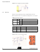
Using the ATAVRAUTO200 Table 2-1. LIN ressources Function Port State Description LIN_NSLP PD2 Low LIN transceiver in Sleep mode High LIN transceiver in normal mode Low Perform MCU reset when NISP Jumper is inserted High No Action NRES_LIN PC6 Note: Note: 2.4.2 GND LIN +VBat Figure 2-3. LIN transceiver and power supply The LIN transceiver undervoltage protection can be disabled by removing the NISP jumper. The NISP jumper has to be removed when programming.
Using the ATAVRAUTO200 Figure 2-4. Power supply measurement through ADC1 2.4.3 Motor relay DC Motor can be operated through a relay. It is supplied with Vbat, -Vbat or 0V. The relay allows the motor to be operated in two rotating directions, or to be stopped. Table 2-2.
Using the ATAVRAUTO200 2.4.4 Current measurement Motor current is measured using a shunt resistor. External differential amplifier (on board) is connected to ADC to measure shunt resistor voltage. Amplifer output (current image voltage) is connected to ADC0 pin for current acquisition AIN1 pin to detect max current peak (compared to AIN0 through internal analog comparator) The current measurement (I) can be performed using the A/D converter. See the ATmega48/88/168 datasheet for how to use the ADC.
Using the ATAVRAUTO200 2.4.6 LED The ATAVRAUTO200 includes one green LED implemented on one I/O pin. It is connected to the “PortD Pin3” of the ATmega48/88/168. To light On the LED, the corresponding port pin must drive a low level. To light Off the LED, the corresponding port pin must drive a high level. Figure 2-8. LED schematic 2.4.7 BOOT An additional jumper (BOOT) has been added. This jumper is available for custom use.
Using the ATAVRAUTO200 2.5.1 Using the ATAVRAUTO900 Adaptator An additionnal adaptator has to be used to program the board using IPS or JTAG mode. The 10 pins connector is used for the JTAGICE mkII device and the 6 pins connector is used for the AVRISP device. To plug the ATAVRAUTO900 connector to the board, the arrow (on the adaptator) has to be in front of the point (on the board). Figure 2-10. ATAVRAUTO900 Connection JTAGICE ISP The arrow has to be in front of the point Table 2-4.
Using the ATAVRAUTO200 2.5.2 Programming with AVR ISP Programmer The AVR ISP programmer is a compact and easy-to-use In-System Programming tool for developing applications with ATmega88. Due to its small size, it is also an excellent tool for field upgrades of existing applications. It is powered by the ATAVRAUTO200 and an additional power supply is thus not required. The AVR ISP programming interface is integrated in AVR Studio.
Using the ATAVRAUTO200 2.6 Debugging 2.6.1 Debugging with AVR JTAGICEmkII The ATAVRAUTO200 can be used for debugging with JTAG ICE MK II. Connect the JTAG ICE mkII as shown in Figure 2-12 for debugging, please refer to AVR Studio Help information.
-12 7698A–AUTO–01/07 ATAVRAUTO200 User Guide
Section 3 Technical Specifications System Unit – Physical Dimensions...............................................L=45 x W=45 x H=8 mm – Weight ........................................................................................................25 g Operating Conditions – Internal Voltage Supply ..... ...................................................................... 5.0V – External Voltage Supply .....................................................................
Section 4 Technical Support For Technical support, please contact avr@atmel.com. When requesting technical support, please include the following information: Which target AVR device is used (complete part number) Target voltage and speed Clock source and fuse setting of the AVR Programming method (ISP, JTAG or specific Boot-Loader) Hardware revisions of the AVR tools, found on the PCB Version number of AVR Studio. This can be found in the AVR Studio help menu.
Section 5 Complete Schematics On the next pages, the following documents of ATAVRAUTO200 are shown: Complete schematics, Bill of materials, Assembly drawing.
Complete Schematics Figure 5-1.
Complete Schematics Figure 5-2.
Complete Schematics Figure 5-3. ATAVRAUTO200 assembly drawing U1 NISP D1 LIN C3 C2 V1.
Atmel Corporation 2325 Orchard Parkway San Jose, CA 95131, USA Tel: 1(408) 441-0311 Fax: 1(408) 487-2600 Regional Headquarters Europe Atmel Sarl Route des Arsenaux 41 Case Postale 80 CH-1705 Fribourg Switzerland Tel: (41) 26-426-5555 Fax: (41) 26-426-5500 Asia Room 1219 Chinachem Golden Plaza 77 Mody Road Tsimshatsui East Kowloon Hong Kong Tel: (852) 2721-9778 Fax: (852) 2722-1369 Japan 9F, Tonetsu Shinkawa Bldg.