Features • High-performance, Low-power Atmel® AVR® 8-bit Microcontroller • Advanced RISC Architecture • • • • • • • • – 131 Powerful Instructions – Most Single-clock Cycle Execution – 32 × 8 General Purpose Working Registers – Fully Static Operation – Up to 20 MIPS Throughput at 20 MHz – On-chip 2-cycle Multiplier High Endurance Non-volatile Memory segments – 16K/32K/64K Bytes of In-System Self-programmable Flash program memory – 512B/1K/2K Bytes EEPROM – 1K/2K/4K Bytes Internal SRAM – Write/Erase Cy
ATmega164P/324P/644P 1. Pin Configurations 1.1 Pinout - PDIP/TQFP/VQFN/QFN/MLF Figure 1-1.
ATmega164P/324P/644P Pinout - DRQFN DRQFN - Pinout ATmega164P Top view Bottom view B2 B14 B3 B4 B1 B14 B2 A16 B13 A16 B13 B3 A15 B12 A15 Table 1-1. A4 B4 A14 B11 A13 B11 A13 B5 A5 A7 B6 A6 A12 B10 A12 B9 A11 B10 B8 A10 B7 A9 A8 A7 B6 A6 A3 B12 A14 A5 B5 A2 B7 A4 A1 B15 A17 A8 A3 A18 B8 A2 A24 B20 B15 A17 A23 B19 A22 A18 B1 B18 A21 B17 A20 B16 A19 A19 B16 A20 B17 A21 B18 A22 B19 A23 B20 A24 A1 A9 Figure 1-2. A11 B9 A10 1.
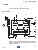
ATmega164P/324P/644P 2. Overview The ATmega164P/324P/644P is a low-power CMOS 8-bit microcontroller based on the AVR enhanced RISC architecture. By executing powerful instructions in a single clock cycle, the ATmega164P/324P/644P achieves throughputs approaching 1 MIPS per MHz allowing the system designer to optimize power consumption versus processing speed. 2.1 Block Diagram Figure 2-1. Block Diagram PA7..0 PB7..
ATmega164P/324P/644P The ATmega164P/324P/644P provides the following features: 16K/32K/64K bytes of In-System Programmable Flash with Read-While-Write capabilities, 512B/1K/2K bytes EEPROM, 1K/2K/4K bytes SRAM, 32 general purpose I/O lines, 32 general purpose working registers, Real Time Counter (RTC), three flexible Timer/Counters with compare modes and PWM, 2 USARTs, a byte oriented 2-wire Serial Interface, a 8-channel, 10-bit ADC with optional differential input stage with programmable gain, programmable
ATmega164P/324P/644P 2.3 2.3.1 Pin Descriptions VCC Digital supply voltage. 2.3.2 GND Ground. 2.3.3 Port A (PA7:PA0) Port A serves as analog inputs to the Analog-to-digital Converter. Port A also serves as an 8-bit bi-directional I/O port with internal pull-up resistors (selected for each bit). The Port A output buffers have symmetrical drive characteristics with both high sink and source capability.
ATmega164P/324P/644P 2.3.7 RESET Reset input. A low level on this pin for longer than the minimum pulse length will generate a reset, even if the clock is not running. The minimum pulse length is given in ”System and Reset Characteristics” on page 331. Shorter pulses are not guaranteed to generate a reset. 2.3.8 XTAL1 Input to the inverting Oscillator amplifier and input to the internal clock operating circuit. 2.3.9 XTAL2 Output from the inverting Oscillator amplifier. 2.3.
ATmega164P/324P/644P 3. About 3.1 Resources A comprehensive set of development tools, application notes and datasheetsare available for download on http://www.atmel.com/avr. 3.2 About Code Examples This documentation contains simple code examples that briefly show how to use various parts of the device. Be aware that not all C compiler vendors include bit definitions in the header files and interrupt handling in C is compiler dependent. Please confirm with the C compiler documentation for more details.
ATmega164P/324P/644P 4. AVR CPU Core 4.1 Overview This section discusses the AVR core architecture in general. The main function of the CPU core is to ensure correct program execution. The CPU must therefore be able to access memories, perform calculations, control peripherals, and handle interrupts. Figure 4-1.
ATmega164P/324P/644P ical ALU operation, two operands are output from the Register File, the operation is executed, and the result is stored back in the Register File – in one clock cycle. Six of the 32 registers can be used as three 16-bit indirect address register pointers for Data Space addressing – enabling efficient address calculations. One of the these address pointers can also be used as an address pointer for look up tables in Flash program memory.
ATmega164P/324P/644P specified in the Instruction Set Reference. This will in many cases remove the need for using the dedicated compare instructions, resulting in faster and more compact code. The Status Register is not automatically stored when entering an interrupt routine and restored when returning from an interrupt. This must be handled by software. 4.3.
ATmega164P/324P/644P 4.4 General Purpose Register File The Register File is optimized for the AVR Enhanced RISC instruction set.
ATmega164P/324P/644P 4.4.1 The X-register, Y-register, and Z-register The registers R26..R31 have some added functions to their general purpose usage. These registers are 16-bit address pointers for indirect addressing of the data space. The three indirect address registers X, Y, and Z are defined as described in Figure 4-3. Figure 4-3.
ATmega164P/324P/644P 4.5.1 SPH and SPL – Stack Pointer High and Stack pointer Low Bit 15 14 13 12 11 10 9 8 0x3E (0x5E) – – – SP12 SP11 SP10 SP9 SP8 SPH 0x3D (0x5D) SP7 SP6 SP5 SP4 SP3 SP2 SP1 SP0 SPL 7 6 5 4 3 2 1 0 Read/Write Initial Value Note: R R R/W R/W R/W R/W R/W R/W R/W R/W R/W R/W R/W R/W 0 0 0 0/0/1(1) 0/1/0(1) 1/0/0(1) 0 0 1 1 1 1 1 1 1 1 1. Initial values respectively for the ATmega164P/324P/644P. Table 4-2. 4.5.
ATmega164P/324P/644P Figure 4-5. The Parallel Instruction Fetches and Instruction Executions T1 T2 T3 T4 clkCPU 1st Instruction Fetch 1st Instruction Execute 2nd Instruction Fetch 2nd Instruction Execute 3rd Instruction Fetch 3rd Instruction Execute 4th Instruction Fetch Figure 4-6 shows the internal timing concept for the Register File. In a single clock cycle an ALU operation using two register operands is executed, and the result is stored back to the destination register. Figure 4-6.
ATmega164P/324P/644P interrupts can then interrupt the current interrupt routine. The I-bit is automatically set when a Return from Interrupt instruction – RETI – is executed. There are basically two types of interrupts. The first type is triggered by an event that sets the Interrupt Flag. For these interrupts, the Program Counter is vectored to the actual Interrupt Vector in order to execute the interrupt handling routine, and hardware clears the corresponding Interrupt Flag.
ATmega164P/324P/644P Assembly Code Example sei ; set Global Interrupt Enable sleep; enter sleep, waiting for interrupt ; note: will enter sleep before any pending ; interrupt(s) C Code Example __enable_interrupt(); /* set Global Interrupt Enable */ __sleep(); /* enter sleep, waiting for interrupt */ /* note: will enter sleep before any pending interrupt(s) */ 4.7.1 Interrupt Response Time The interrupt execution response for all the enabled AVR interrupts is five clock cycles minimum.
ATmega164P/324P/644P 5. AVR Memories 5.1 Overview This section describes the different memories in the ATmega164P/324P/644P. The AVR architecture has two main memory spaces, the Data Memory and the Program Memory space. In addition, the ATmega164P/324P/644P features an EEPROM Memory for data storage. All three memory spaces are linear and regular. 5.
ATmega164P/324P/644P Figure 5-1. Program Memory Map Program Memory 0x0000 Application Flash Section Boot Flash Section 0x1FFF 5.3 SRAM Data Memory Figure 5-2 shows how the ATmega164P/324P/644P SRAM Memory is organized. The ATmega164P/324P/644P is a complex microcontroller with more peripheral units than can be supported within the 64 location reserved in the Opcode for the IN and OUT instructions.
ATmega164P/324P/644P The 32 general purpose working registers, 64 I/O registers, 160 Extended I/O Registers and the 1024/2048/4096 bytes of internal data SRAM in the ATmega164P/324P/644P are all accessible through all these addressing modes. The Register File is described in ”General Purpose Register File” on page 12. Figure 5-2. Data Memory Map for ATmega164P/324P/644P. Data Memory 32 Registers 64 I/O Registers 160 Ext I/O Reg.
ATmega164P/324P/644P 5.4 EEPROM Data Memory The ATmega164P/324P/644P contains 512B/1K/2K bytes of data EEPROM memory. It is organized as a separate data space, in which single bytes can be read and written. The EEPROM has an endurance of at least 100,000 write/erase cycles. The access between the EEPROM and the CPU is described in the following, specifying the EEPROM Address Registers, the EEPROM Data Register, and the EEPROM Control Register.
ATmega164P/324P/644P 5.5 I/O Memory The I/O space definition of the ATmega164P/324P/644P is shown in ”Register Summary” on page 413. All ATmega164P/324P/644P I/Os and peripherals are placed in the I/O space. All I/O locations may be accessed by the LD/LDS/LDD and ST/STS/STD instructions, transferring data between the 32 general purpose working registers and the I/O space. I/O Registers within the address range 0x00 - 0x1F are directly bit-accessible using the SBI and CBI instructions.
ATmega164P/324P/644P 5.6 5.6.
ATmega164P/324P/644P While EEPE is set, any write to EEPMn will be ignored. During reset, the EEPMn bits will be reset to 0b00 unless the EEPROM is busy programming. Table 5-1. EEPROM Mode Bits EEPM1 EEPM0 Programming Time 0 0 3.4 ms Erase and Write in one operation (Atomic Operation) 0 1 1.8 ms Erase Only 1 0 1.
ATmega164P/324P/644P When the write access time has elapsed, the EEPE bit is cleared by hardware. The user software can poll this bit and wait for a zero before writing the next byte. When EEPE has been set, the CPU is halted for two cycles before the next instruction is executed. • Bit 0 – EERE: EEPROM Read Enable The EEPROM Read Enable Signal EERE is the read strobe to the EEPROM.
ATmega164P/324P/644P The following code examples show one assembly and one C function for writing to the EEPROM. The examples assume that interrupts are controlled (for example by disabling interrupts globally) so that no interrupts will occur during execution of these functions. The examples also assume that no Flash Boot Loader is present in the software. If such code is present, the EEPROM write function must also wait for any ongoing SPM command to finish.
ATmega164P/324P/644P The next code examples show assembly and C functions for reading the EEPROM. The examples assume that interrupts are controlled so that no interrupts will occur during execution of these functions.
ATmega164P/324P/644P 5.6.4 GPIOR2 – General Purpose I/O Register 2 Bit 5.6.5 7 5 4 3 2 1 0 MSB Read/Write R/W R/W R/W R/W R/W R/W R/W R/W Initial Value 0 0 0 0 0 0 0 0 LSB 5 4 3 2 1 GPIOR2 GPIOR1 – General Purpose I/O Register 1 Bit 5.6.
ATmega164P/324P/644P 6. System Clock and Clock Options 6.1 Clock Systems and their Distribution Figure 6-1 presents the principal clock systems in the AVR and their distribution. All of the clocks need not be active at a given time. In order to reduce power consumption, the clocks to modules not being used can be halted by using different sleep modes, as described in ”Power Management and Sleep Modes” on page 42. The clock systems are detailed below. Figure 6-1.
ATmega164P/324P/644P 6.1.3 Flash Clock – clkFLASH The Flash clock controls operation of the Flash interface. The Flash clock is usually active simultaneously with the CPU clock. 6.1.4 Asynchronous Timer Clock – clkASY The Asynchronous Timer clock allows the Asynchronous Timer/Counter to be clocked directly from an external clock or an external 32 kHz clock crystal. The dedicated clock domain allows using this Timer/Counter as a real-time counter even when the device is in sleep mode. 6.1.
ATmega164P/324P/644P selectable delays are shown in Table 6-2. The frequency of the Watchdog Oscillator is voltage dependent as shown in ”Typical Characteristics” on page 338. Table 6-2. Number of Watchdog Oscillator Cycles Typ Time-out (VCC = 5.0V) Typ Time-out (VCC = 3.0V) Number of Cycles 0 ms 0 ms 0 4.1 ms 4.3 ms 512 65 ms 69 ms 8K (8,192) Main purpose of the delay is to keep the AVR in reset until it is supplied with minimum Vcc.
ATmega164P/324P/644P 6.3 Low Power Crystal Oscillator This Crystal Oscillator is a low power oscillator, with reduced voltage swing on the XTAL2 output. It gives the lowest power consumption, but is not capable of driving other clock inputs, and may be more susceptible to noise in noisy environments. In these cases, refer to the ”Full Swing Crystal Oscillator” on page 33. Some initial guidelines for choosing capacitors for use with crystals are given in Table 6-3.
ATmega164P/324P/644P Table 6-4. Start-up Times for the Low Power Crystal Oscillator Clock Selection (Continued) Start-up Time from Power-down and Power-save Additional Delay from Reset (VCC = 5.0V) CKSEL0 SUT1..0 Crystal Oscillator, BOD enabled 16K CK 14CK 1 01 Crystal Oscillator, fast rising power 16K CK 14CK + 4.1 ms 1 10 Crystal Oscillator, slowly rising power 16K CK 14CK + 65 ms 1 11 Oscillator Source / Power Conditions Notes: 6.4 1.
ATmega164P/324P/644P Table 6-6. Start-up Times for the Full Swing Crystal Oscillator Clock Selection Start-up Time from Power-down and Power-save Additional Delay from Reset (VCC = 5.0V) CKSEL0 SUT1..0 Ceramic resonator, fast rising power 1K CK 14CK + 4.1 ms(2) 0 11 Ceramic resonator, slowly rising power 1K CK 14CK + 65 ms(2) 1 00 Crystal Oscillator, BOD enabled 16K CK 14CK 1 01 Crystal Oscillator, fast rising power 16K CK 14CK + 4.
ATmega164P/324P/644P The capacitance (Ce +Ci) needed at each TOSC pin can be calculated by using: C = 2 ⋅ CL – C s where: – Ce - is optional external capacitors as described in Figure 8-2 on page29 – Ci - is the pin capacitance in table 8-8 on page 33 – CL - is the load capacitance for a 32.768 kHz crystal specified by the crystal vendor – CS - is the total stray capacitance for one TOSC pin. Crystals specifying load capacitance (CL) higher than 8.
ATmega164P/324P/644P 6.6 Calibrated Internal RC Oscillator By default, the Internal RC Oscillator provides an approximate 8 MHz clock. Though voltage and temperature dependent, this clock can be very accurately calibrated by the the user. See Table 25-4 on page 330 and ”Internal Oscillator Speed” on page 356 and page 380 for more details. The device is shipped with the CKDIV8 Fuse programmed. See ”System Clock Prescaler” on page 38 for more details.
ATmega164P/324P/644P 6.7 128 kHz Internal Oscillator The 128 kHz internal Oscillator is a low power Oscillator providing a clock of 128 kHz. The frequency is nominal at 3V and 25°C. This clock may be select as the system clock by programming the CKSEL Fuses to “0011” as shown in Table 6-12. Table 6-12. Note: 128 kHz Internal Oscillator Operating Modes(2) Nominal Frequency CKSEL3..0 128 kHz 0011 1.
ATmega164P/324P/644P Table 6-15. Start-up Times for the External Clock Selection Start-up Time from Powerdown and Power-save Additional Delay from Reset (VCC = 5.0V) SUT1..0 BOD enabled 6 CK 14CK 00 Fast rising power 6 CK 14CK + 4.1 ms 01 Slowly rising power 6 CK 14CK + 65 ms 10 Power Conditions Reserved 11 When applying an external clock, it is required to avoid sudden changes in the applied clock frequency to ensure stable operation of the MCU.
ATmega164P/324P/644P neither the clock frequency corresponding to the previous setting, nor the clock frequency corresponding to the new setting. The ripple counter that implements the prescaler runs at the frequency of the undivided clock, which may be faster than the CPU's clock frequency. Hence, it is not possible to determine the state of the prescaler - even if it were readable, and the exact time it takes to switch from one clock division to the other cannot be exactly predicted.
ATmega164P/324P/644P 6.12 6.12.1 Register Description OSCCAL – Oscillator Calibration Register Bit (0x66) Read/Write 7 6 5 4 3 2 1 0 CAL7 CAL6 CAL5 CAL4 CAL3 CAL2 CAL1 CAL0 R/W R/W R/W R/W R/W R/W R/W R/W Initial Value OSCCAL Device Specific Calibration Value • Bits 7:0 – CAL7:0: Oscillator Calibration Value The Oscillator Calibration Register is used to trim the Calibrated Internal RC Oscillator to remove process variations from the oscillator frequency.
ATmega164P/324P/644P The CKDIV8 Fuse determines the initial value of the CLKPS bits. If CKDIV8 is unprogrammed, the CLKPS bits will be reset to “0000”. If CKDIV8 is programmed, CLKPS bits are reset to “0011”, giving a division factor of 8 at start up. This feature should be used if the selected clock source has a higher frequency than the maximum frequency of the device at the present operating conditions. Note that any value can be written to the CLKPS bits regardless of the CKDIV8 Fuse setting.
ATmega164P/324P/644P 7. Power Management and Sleep Modes 7.1 Overview Sleep modes enable the application to shut down unused modules in the MCU, thereby savingpower. The AVR provides various sleep modes allowing the user to tailor the power consumption to the application’s requirements. When enabled, the Brown-out Detector (BOD) actively monitors the power supply voltage during the sleep periods. To further save power, it is possible to disable the BOD in some sleep modes.
ATmega164P/324P/644P 7.3 BOD Disable When the Brown-out Detector (BOD) is enabled by BODLEVEL fuses, Table 24-3 on page 294, the BOD is actively monitoring the power supply voltage during a sleep period. To save power, it is possible to disable the BOD by software for some of the sleep modes, see Table 7-1 on page 42. The sleep mode power consumption will then be at the same level as when BOD is globally disabled by fuses.
ATmega164P/324P/644P 7.6 Power-down Mode When the SM2..0 bits are written to 010, the SLEEP instruction makes the MCU enter Powerdown mode. In this mode, the external Oscillator is stopped, while the external interrupts, the 2wire Serial Interface, and the Watchdog continue operating (if enabled).
ATmega164P/324P/644P 7.10 Power Reduction Register The Power Reduction Register(PRR), see ”PRR – Power Reduction Register” on page 48, provides a method to stop the clock to individual peripherals to reduce power consumption. The current state of the peripheral is frozen and the I/O registers can not be read or written. Resources used by the peripheral when stopping the clock will remain occupied, hence the peripheral should in most cases be disabled before stopping the clock.
ATmega164P/324P/644P 7.11.5 Watchdog Timer If the Watchdog Timer is not needed in the application, the module should be turned off. If the Watchdog Timer is enabled, it will be enabled in all sleep modes, and hence, always consume power. In the deeper sleep modes, this will contribute significantly to the total current consumption. Refer to ”Interrupts” on page 61 for details on how to configure the Watchdog Timer. 7.11.
ATmega164P/324P/644P 7.12 7.12.1 Register Description SMCR – Sleep Mode Control Register The Sleep Mode Control Register contains control bits for power management. Bit 7 6 5 4 3 2 1 0 0x33 (0x53) – – – – SM2 SM1 SM0 SE Read/Write R R R R R/W R/W R/W R/W Initial Value 0 0 0 0 0 0 0 0 SMCR • Bits 3, 2, 1 – SM2:0: Sleep Mode Select Bits 2, 1, and 0 These bits select between the five available sleep modes as shown in Table 7-2. Table 7-2.
ATmega164P/324P/644P 7.12.2 MCUCR – MCU Control Register Bit 7 6 5 4 3 2 1 0 0x35 (0x55) JTD BODS BODSE PUD – – IVSEL IVCE Read/Write R/W R R R/W R R R/W R/W Initial Value 0 0 0 0 0 0 0 0 MCUCR • Bit 6 – BODS: BOD Sleep The BODS bit must be written to logic one in order to turn off BOD during sleep, see Table 7-1 on page 42. Writing to the BODS bit is controlled by a timed sequence and an enable bit, BODSE in MCUCR.
ATmega164P/324P/644P • Bit 2 - PRSPI: Power Reduction Serial Peripheral Interface Writing a logic one to this bit shuts down the Serial Peripheral Interface by stopping the clock to the module. When waking up the SPI again, the SPI should be re initialized to ensure proper operation. • Bit 1 - PRUSART0: Power Reduction USART0 Writing a logic one to this bit shuts down the USART0 by stopping the clock to the module.
ATmega164P/324P/644P 8. System Control and Reset 8.1 Resetting the AVR During reset, all I/O Registers are set to their initial values, and the program starts execution from the Reset Vector. The instruction placed at the Reset Vector must be a JMP – Absolute Jump – instruction to the reset handling routine. If the program never enables an interrupt source, the Interrupt Vectors are not used, and regular program code can be placed at these locations.
ATmega164P/324P/644P Figure 8-1. Reset Logic DATA BUS PORF BORF EXTRF WDRF JTRF MCU Status Register (MCUSR) Power-on Reset Circuit Brown-out Reset Circuit BODLEVEL [2..0] Pull-up Resistor SPIKE FILTER JTAG Reset Register Watchdog Oscillator Clock Generator CK Delay Counters TIMEOUT CKSEL[3:0] SUT[1:0] 8.3 Power-on Reset A Power-on Reset (POR) pulse is generated by an On-chip detection circuit. The detection level is defined in ”System and Reset Characteristics” on page 331.
ATmega164P/324P/644P Figure 8-2. MCU Start-up, RESET Tied to VCC VCC RESET VPOT VRST tTOUT TIME-OUT INTERNAL RESET Figure 8-3. MCU Start-up, RESET Extended Externally VCC RESET VPOT VRST tTOUT TIME-OUT INTERNAL RESET 8.4 External Reset An External Reset is generated by a low level on the RESET pin. Reset pulses longer than the minimum pulse width (see ”System and Reset Characteristics” on page 331) will generate a reset, even if the clock is not running.
ATmega164P/324P/644P 8.5 Brown-out Detection ATmega164P/324P/644P has an On-chip Brown-out Detection (BOD) circuit for monitoring the VCC level during operation by comparing it to a fixed trigger level. The trigger level for the BOD can be selected by the BODLEVEL Fuses. The trigger level has a hysteresis to ensure spike free Brown-out Detection. The hysteresis on the detection level should be interpreted as VBOT+ = VBOT + VHYST/2 and VBOT- = VBOT - VHYST/2.
ATmega164P/324P/644P 8.7 Internal Voltage Reference ATmega164P/324P/644P features an internal bandgap reference. This reference is used for Brown-out Detection, and it can be used as an input to the Analog Comparator or the ADC. 8.7.1 Voltage Reference Enable Signals and Start-up Time The voltage reference has a start-up time that may influence the way it should be used. The start-up time is given in ”System and Reset Characteristics” on page 331. To save power, the reference is not always turned on.
ATmega164P/324P/644P 8.8 8.8.1 Watchdog Timer Features • Clocked from separate On-chip Oscillator • 3 Operating modes – Interrupt – System Reset – Interrupt and System Reset • Selectable Time-out period from 16 ms to 8s • Possible Hardware fuse Watchdog always on (WDTON) for fail-safe mode 8.8.2 Overview ATmega164P/324P/644P has an Enhanced Watchdog Timer (WDT). The WDT is a timer counting cycles of a separate on-chip 128 kHz oscillator.
ATmega164P/324P/644P 1. In the same operation, write a logic one to the Watchdog change enable bit (WDCE) and WDE. A logic one must be written to WDE regardless of the previous value of the WDE bit. 2. Within the next four clock cycles, write the WDE and Watchdog prescaler bits (WDP) as desired, but with the WDCE bit cleared. This must be done in one operation. The following code example shows one assembly and one C function for turning off the Watchdog Timer.
ATmega164P/324P/644P Note: If the Watchdog is accidentally enabled, for example by a runaway pointer or brown-out condition, the device will be reset and the Watchdog Timer will stay enabled. If the code is not set up to handle the Watchdog, this might lead to an eternal loop of time-out resets. To avoid this situation, the application software should always clear the Watchdog System Reset Flag (WDRF) and the WDE control bit in the initialisation routine, even if the Watchdog is not in use.
ATmega164P/324P/644P 8.9 8.9.1 Register Description MCUSR – MCU Status Register The MCU Status Register provides information on which reset source caused an MCU reset. Bit 7 6 5 4 3 2 1 0 0x34 (0x54) – – – JTRF WDRF BORF EXTRF PORF Read/Write R R R R/W R/W R/W R/W R/W Initial Value 0 0 0 MCUSR See Bit Description • Bit 4 – JTRF: JTAG Reset Flag This bit is set if a reset is being caused by a logic one in the JTAG Reset Register selected by the JTAG instruction AVR_RESET.
ATmega164P/324P/644P 8.9.2 WDTCSR – Watchdog Timer Control Register Bit 7 6 5 4 3 2 1 0 (0x60) WDIF WDIE WDP3 WDCE WDE WDP2 WDP1 WDP0 Read/Write R/W R/W R/W R/W R/W R/W R/W R/W Initial Value 0 0 0 0 X 0 0 0 WDTCSR • Bit 7 - WDIF: Watchdog Interrupt Flag This bit is set when a time-out occurs in the Watchdog Timer and the Watchdog Timer is configured for interrupt. WDIF is cleared by hardware when executing the corresponding interrupt handling vector.
ATmega164P/324P/644P • Bit 5, 2:0 - WDP3:0: Watchdog Timer Prescaler 3, 2, 1 and 0 The WDP3:0 bits determine the Watchdog Timer prescaling when the Watchdog Timer is running. The different prescaling values and their corresponding time-out periods are shown in Table 8-2 on page 60. . Table 8-2. Watchdog Timer Prescale Select WDP3 WDP2 WDP1 WDP0 Number of WDT Oscillator Cycles Typical Time-out at VCC = 5.
ATmega164P/324P/644P 9. Interrupts 9.1 Overview This section describes the specifics of the interrupt handling as performed in ATmega164P/324P/644P. For a general explanation of the AVR interrupt handling, refer to ”Reset and Interrupt Handling” on page 15. 9.2 Interrupt Vectors in ATmega164P/324P/644P Table 9-1. Vector No.
ATmega164P/324P/644P Table 9-1. Vector No. Reset and Interrupt Vectors (Continued) Program Address(2) Source Interrupt Definition 28 $0036 SPM_READY Store Program Memory Ready 29 $0038 USART1_RX USART1 Rx Complete 30 $003A USART1_UDRE USART1 Data Register Empty 31 $003C USART1_TX USART1 Tx Complete Notes: 1. When the BOOTRST Fuse is programmed, the device will jump to the Boot Loader address at reset, see ”Memory Programming” on page 293. 2.
ATmega164P/324P/644P 0x0022 0x0024 0x0026 0x0028 0x002A 0x002C 0x002E 0x0030 0x0032 0x0034 0x0036 0x0038 0x003A 0x003C ; 0x003E RESET: jmp jmp jmp jmp jmp jmp jmp jmp jmp jmp jmp jmp jmp jmp TIM0_COMPB TIM0_OVF SPI_STC USART0_RXC USART0_UDRE USART0_TXC ANA_COMP ADC EE_RDY TWI SPM_RDY USART1_RXC USART1_UDRE USART1_TXC ; ; ; ; ; ; ; ; ; ; ; ; ; ; ldi r16, high(RAMEND) SPH,r16 ; Main program start 0x003F out 0x0040 ldi 0x0041 0x0042 0x0043 ... out sei ... ...
ATmega164P/324P/644P 0x00004 jmp EXT_INT1 ; IRQ1 Handler ... ... ... ; 0x00036 jmp SPM_RDY ; SPM Ready Handler ; .
ATmega164P/324P/644P 9.3 9.3.1 Register Description MCUCR – MCU Control Register Bit 7 6 5 4 3 2 1 0 0x35 (0x55) JTD BODS BODSE PUD – – IVSEL IVCE Read/Write R/W R R R/W R R R/W R/W Initial Value 0 0 0 0 0 0 0 0 MCUCR • Bit 1 – IVSEL: Interrupt Vector Select When the IVSEL bit is cleared (zero), the Interrupt Vectors are placed at the start of the Flash memory.
ATmega164P/324P/644P Assembly Code Example Move_interrupts: ; Get MCUCR in r16, MCUCR mov r17, r16 ; Enable change of Interrupt Vectors ori r16, (1<
ATmega164P/324P/644P 10. External Interrupts 10.1 Overview The External Interrupts are triggered by the INT2:0 pin or any of the PCINT31:0 pins. Observe that, if enabled, the interrupts will trigger even if the INT2:0 or PCINT31:0 pins are configured as outputs. This feature provides a way of generating a software interrupt.
ATmega164P/324P/644P pletion of the currently executing instruction to generate an interrupt. If enabled, a level triggered interrupt will generate an interrupt request as long as the pin is held low. When changing the ISCn bit, an interrupt can occur. Therefore, it is recommended to first disable INTn by clearing its Interrupt Enable bit in the EIMSK Register. Then, the ISCn bit can be changed.
ATmega164P/324P/644P 10.2.4 PCICR – Pin Change Interrupt Control Register Bit 7 6 5 4 3 2 1 0 (0x68) – – – – PCIE3 PCIE2 PCIE1 PCIE0 Read/Write R R R R R/W R/W R/W R/W Initial Value 0 0 0 0 0 0 0 0 PCICR • Bit 3 – PCIE3: Pin Change Interrupt Enable 3 When the PCIE3 bit is set (one) and the I-bit in the Status Register (SREG) is set (one), pin change interrupt 3 is enabled. Any change on any enabled PCINT31..24 pin will cause an interrupt.
ATmega164P/324P/644P • Bit 1 – PCIF1: Pin Change Interrupt Flag 1 When a logic change on any PCINT15..8 pin triggers an interrupt request, PCIF1 becomes set (one). If the I-bit in SREG and the PCIE1 bit in EIMSK are set (one), the MCU will jump to the corresponding Interrupt Vector. The flag is cleared when the interrupt routine is executed. Alternatively, the flag can be cleared by writing a logical one to it. • Bit 0 – PCIF0: Pin Change Interrupt Flag 0 When a logic change on any PCINT7..
ATmega164P/324P/644P 10.2.9 PCMSK0 – Pin Change Mask Register 0 Bit 7 6 5 4 3 2 1 0 (0x6B) PCINT7 PCINT6 PCINT5 PCINT4 PCINT3 PCINT2 PCINT1 PCINT0 Read/Write R/W R/W R/W R/W R/W R/W R/W R/W Initial Value 0 0 0 0 0 0 0 0 PCMSK0 • Bit 7:0 – PCINT7:0: Pin Change Enable Mask 7..0 Each PCINT7:0 bit selects whether pin change interrupt is enabled on the corresponding I/O pin.
ATmega164P/324P/644P 11. I/O-Ports 11.1 Overview All AVR ports have true Read-Modify-Write functionality when used as general digital I/O ports. This means that the direction of one port pin can be changed without unintentionally changing the direction of any other pin with the SBI and CBI instructions. The same applies when changing drive value (if configured as output) or enabling/disabling of pull-up resistors (if configured as input).
ATmega164P/324P/644P Note that enabling the alternate function of some of the port pins does not affect the use of the other pins in the port as general digital I/O. 11.2 Ports as General Digital I/O The ports are bi-directional I/O ports with optional internal pull-ups. Figure 11-2 shows a functional description of one I/O-port pin, here generically called Pxn. Figure 11-2.
ATmega164P/324P/644P If PORTxn is written logic one when the pin is configured as an output pin, the port pin is driven high (one). If PORTxn is written logic zero when the pin is configured as an output pin, the port pin is driven low (zero). 11.2.2 Toggling the Pin Writing a logic one to PINxn toggles the value of PORTxn, independent on the value of DDRxn. Note that the SBI instruction can be used to toggle one single bit in a port. 11.2.
ATmega164P/324P/644P Figure 11-3. Synchronization when Reading an Externally Applied Pin value SYSTEM CLK INSTRUCTIONS XXX XXX in r17, PINx SYNC LATCH PINxn r17 0x00 0xFF t pd, max t pd, min Consider the clock period starting shortly after the first falling edge of the system clock. The latch is closed when the clock is low, and goes transparent when the clock is high, as indicated by the shaded region of the “SYNC LATCH” signal. The signal value is latched when the system clock goes low.
ATmega164P/324P/644P Assembly Code Example(1) ... ; Define pull-ups and set outputs high ; Define directions for port pins ldi r16,(1<
ATmega164P/324P/644P 11.2.6 Unconnected Pins If some pins are unused, it is recommended to ensure that these pins have a defined level. Even though most of the digital inputs are disabled in the deep sleep modes as described above, floating inputs should be avoided to reduce current consumption in all other modes where the digital inputs are enabled (Reset, Active mode and Idle mode). The simplest method to ensure a defined level of an unused pin, is to enable the internal pull-up.
ATmega164P/324P/644P 11.3 Alternate Port Functions Most port pins have alternate functions in addition to being general digital I/Os. Figure 11-5 shows how the port pin control signals from the simplified Figure 11-2 on page 73 can be overridden by alternate functions. The overriding signals may not be present in all port pins, but the figure serves as a generic description applicable to all port pins in the AVR microcontroller family. Figure 11-5.
ATmega164P/324P/644P Table 11-2 summarizes the function of the overriding signals. The pin and port indexes from Figure 11-5 are not shown in the succeeding tables. The overriding signals are generated internally in the modules having the alternate function. Table 11-2. Generic Description of Overriding Signals for Alternate Functions Signal Name Full Name Description PUOE Pull-up Override Enable If this signal is set, the pull-up enable is controlled by the PUOV signal.
ATmega164P/324P/644P 11.3.1 Alternate Functions of Port A The Port A pins with alternate functions are shown in Table 11-3. Table 11-3.
ATmega164P/324P/644P Table 11-4 on page 81 and Table 11-5 on page 81 relates the alternate functions of Port A to the overriding signals shown in Figure 11-5 on page 78. Table 11-4.
ATmega164P/324P/644P 11.3.2 Alternate Functions of Port B The Port B pins with alternate functions are shown in Table 11-6. Table 11-6.
ATmega164P/324P/644P • MOSI/PCINT13 – Port B, Bit 5 MOSI: SPI Master Data output, Slave Data input for SPI channel. When the SPI is enabled as a slave, this pin is configured as an input regardless of the setting of DDB5. When the SPI is enabled as a master, the data direction of this pin is controlled by DDB5. When the pin is forced to be an input, the pull-up can still be controlled by the PORTB5 bit. PCINT13, Pin Change Interrupt source 13: The PB5 pin can serve as an external interrupt source.
ATmega164P/324P/644P • T0/XCK0/PCINT8, Bit 0 T0, Timer/Counter0 counter source. XCK0, USART0 External clock. The Data Direction Register (DDB0) controls whether the clock is output (DDD0 set “one”) or input (DDD0 cleared). The XCK0 pin is active only when the USART0 operates in Synchronous mode. PCINT8, Pin Change Interrupt source 8: The PB0 pin can serve as an external interrupt source.
ATmega164P/324P/644P 11.3.3 Alternate Functions of Port C The Port C pins with alternate functions are shown in Table 11-9. Table 11-9.
ATmega164P/324P/644P • TMS/PCINT19 – Port C, Bit 3 TMS, JTAG Test Mode Select. PCINT19, Pin Change Interrupt source 19: The PC3 pin can serve as an external interrupt source. • TCK/PCINT18 – Port C, Bit 2 TCK, JTAG Test Clock. PCINT18, Pin Change Interrupt source 18: The PC2 pin can serve as an external interrupt source. • SDA/PCINT17 – Port C, Bit 1 SDA, 2-wire Serial Bus Data Input/Output Line. PCINT17, Pin Change Interrupt source 17: The PC1 pin can serve as an external interrupt source.
ATmega164P/324P/644P Table 11-11. Overriding Signals for Alternate Functions in PC3:PC0 11.3.
ATmega164P/324P/644P The alternate pin configuration is as follows: • OC2A/PCINT31 – Port D, Bit 7 OC2A, Output Compare Match A output: The PD7 pin can serve as an external output for the Timer/Counter2 Output Compare A. The pin has to be configured as an output (DDD7 set (one)) to serve this function. The OC2A pin is also the output pin for the PWM mode timer function. PCINT31, Pin Change Interrupt Source 31:The PD7 pin can serve as an external interrupt source.
ATmega164P/324P/644P • INT0/RXD1/PCINT26 – Port D, Bit 2 INT0, External Interrupt source 0. The PD2 pin can serve as an external interrupt source to the MCU. RXD1, RXD0, Receive Data (Data input pin for the USART1). When the USART1 receiver is enabled this pin is configured as an input regardless of the value of DDD2. When the USART forces this pin to be an input, the pull-up can still be controlled by the PORTD2 bit.
ATmega164P/324P/644P Table 11-14.
ATmega164P/324P/644P Register Description 11.3.5 MCUCR – MCU Control Register Bit 7 6 5 4 3 2 1 0 0x35 (0x55) JTD BODS BODSE PUD – – IVSEL IVCE Read/Write R/W R R R/W R R R/W R/W Initial Value 0 0 0 0 0 0 0 0 MCUCR • Bit 4 – PUD: Pull-up Disable When this bit is written to one, the pull-ups in the I/O ports are disabled even if the DDxn and PORTxn Registers are configured to enable the pull-ups ({DDxn, PORTxn} = 0b01).
ATmega164P/324P/644P 11.3.12 PORTC – Port C Data Register Bit 11.3.13 7 6 5 4 3 2 1 0 0x08 (0x28) PORTC7 PORTC6 PORTC5 PORTC4 PORTC3 PORTC2 PORTC1 PORTC0 Read/Write R/W R/W R/W R/W R/W R/W R/W R/W Initial Value 0 0 0 0 0 0 0 0 DDRC – Port C Data Direction Register Bit 11.3.
ATmega164P/324P/644P 12. 8-bit Timer/Counter0 with PWM 12.1 Features • • • • • • • 12.2 Two Independent Output Compare Units Double Buffered Output Compare Registers Clear Timer on Compare Match (Auto Reload) Glitch Free, Phase Correct Pulse Width Modulator (PWM) Variable PWM Period Frequency Generator Three Independent Interrupt Sources (TOV0, OCF0A, and OCF0B) Overview Timer/Counter0 is a general purpose 8-bit Timer/Counter module, with two independent Output Compare Units, and with PWM support.
ATmega164P/324P/644P uses to increment (or decrement) its value. The Timer/Counter is inactive when no clock source is selected. The output from the Clock Select logic is referred to as the timer clock (clkT0). The double buffered Output Compare Registers (OCR0A and OCR0B) are compared with the Timer/Counter value at all times. The result of the compare can be used by the Waveform Generator to generate a PWM or variable frequency output on the Output Compare pins (OC0A and OC0B). See Section “12.
ATmega164P/324P/644P count Increment or decrement TCNT0 by 1. direction Select between increment and decrement. clear Clear TCNT0 (set all bits to zero). clkTn Timer/Counter clock, referred to as clkT0 in the following. top Signalize that TCNT0 has reached maximum value. bottom Signalize that TCNT0 has reached minimum value (zero). Depending of the mode of operation used, the counter is cleared, incremented, or decremented at each timer clock (clkT0).
ATmega164P/324P/644P Figure 12-3. Output Compare Unit, Block Diagram DATA BUS OCRnx TCNTn = (8-bit Comparator ) OCFnx (Int.Req.) top bottom Waveform Generator OCnx FOCn WGMn1:0 COMnX1:0 The OCR0x Registers are double buffered when using any of the Pulse Width Modulation (PWM) modes. For the normal and Clear Timer on Compare (CTC) modes of operation, the double buffering is disabled.
ATmega164P/324P/644P generation. Similarly, do not write the TCNT0 value equal to BOTTOM when the counter is down-counting. The setup of the OC0x should be performed before setting the Data Direction Register for the port pin to output. The easiest way of setting the OC0x value is to use the Force Output Compare (FOC0x) strobe bits in Normal mode. The OC0x Registers keep their values even when changing between Waveform Generation modes.
ATmega164P/324P/644P 12.6.1 Compare Output Mode and Waveform Generation The Waveform Generator uses the COM0x1:0 bits differently in Normal, CTC, and PWM modes. For all modes, setting the COM0x1:0 = 0 tells the Waveform Generator that no action on the OC0x Register is to be performed on the next Compare Match. For compare output actions in the non-PWM modes refer to Table 12-2 on page 104. For fast PWM mode, refer to Table 12-3 on page 104, and for phase correct PWM refer to Table 12-4 on page 105.
ATmega164P/324P/644P Figure 12-5. CTC Mode, Timing Diagram OCnx Interrupt Flag Set TCNTn OCn (Toggle) Period (COMnx1:0 = 1) 1 2 3 4 An interrupt can be generated each time the counter value reaches the TOP value by using the OCF0A Flag. If the interrupt is enabled, the interrupt handler routine can be used for updating the TOP value.
ATmega164P/324P/644P PWM mode is shown in Figure 12-6. The TCNT0 value is in the timing diagram shown as a histogram for illustrating the single-slope operation. The diagram includes non-inverted and inverted PWM outputs. The small horizontal line marks on the TCNT0 slopes represent Compare Matches between OCR0x and TCNT0. Figure 12-6.
ATmega164P/324P/644P feature is similar to the OC0A toggle in CTC mode, except the double buffer feature of the Output Compare unit is enabled in the fast PWM mode. 12.7.4 Phase Correct PWM Mode The phase correct PWM mode (WGM02:0 = 1 or 5) provides a high resolution phase correct PWM waveform generation option. The phase correct PWM mode is based on a dual-slope operation. The counter counts repeatedly from BOTTOM to TOP and then from TOP to BOTTOM.
ATmega164P/324P/644P one allows the OC0A pin to toggle on Compare Matches if the WGM02 bit is set. This option is not available for the OC0B pin (See Table 12-4 on page 105). The actual OC0x value will only be visible on the port pin if the data direction for the port pin is set as output.
ATmega164P/324P/644P Figure 12-9. Timer/Counter Timing Diagram, with Prescaler (fclk_I/O/8) clkI/O clkTn (clkI/O /8) TCNTn MAX - 1 MAX BOTTOM BOTTOM + 1 TOVn Figure 12-10 shows the setting of OCF0B in all modes and OCF0A in all modes except CTC mode and PWM mode, where OCR0A is TOP. Figure 12-10.
ATmega164P/324P/644P 12.9 12.9.1 Register Description TCCR0A – Timer/Counter Control Register A Bit 7 6 5 4 3 2 1 0 0x24 (0x44) COM0A1 COM0A0 COM0B1 COM0B0 – – WGM01 WGM00 Read/Write R/W R/W R/W R/W R R R/W R/W Initial Value 0 0 0 0 0 0 0 0 TCCR0A • Bits 7:6 – COM0A1:0: Compare Match Output A Mode These bits control the Output Compare pin (OC0A) behavior.
ATmega164P/324P/644P Table 12-4. Compare Output Mode, Phase Correct PWM Mode(1) COM0A1 COM0A0 0 0 Normal port operation, OC0A disconnected. 0 1 WGM02 = 0: Normal Port Operation, OC0A Disconnected. WGM02 = 1: Toggle OC0A on Compare Match. 1 0 Clear OC0A on Compare Match when up-counting. Set OC0A on Compare Match when down-counting. 1 1 Set OC0A on Compare Match when up-counting. Clear OC0A on Compare Match when down-counting. Note: Description 1.
ATmega164P/324P/644P Table 12-7 on page 106 shows the COM0B1:0 bit functionality when the WGM02:0 bits are set to phase correct PWM mode. Compare Output Mode, Phase Correct PWM Mode(1) Table 12-7. COM0B1 COM0B0 0 0 Normal port operation, OC0B disconnected. 0 1 Reserved 1 0 Clear OC0B on Compare Match when up-counting. Set OC0B on Compare Match when down-counting. 1 1 Set OC0B on Compare Match when up-counting. Clear OC0B on Compare Match when down-counting. Note: Description 1.
ATmega164P/324P/644P 12.9.2 TCCR0B – Timer/Counter Control Register B Bit 7 6 5 4 3 2 1 0 0x25 (0x45) FOC0A FOC0B – – WGM02 CS02 CS01 CS00 Read/Write W W R R R/W R/W R/W R/W Initial Value 0 0 0 0 0 0 0 0 TCCR0B • Bit 7 – FOC0A: Force Output Compare A The FOC0A bit is only active when the WGM bits specify a non-PWM mode. However, for ensuring compatibility with future devices, this bit must be set to zero when TCCR0B is written when operating in PWM mode.
ATmega164P/324P/644P • Bits 2:0 – CS02:0: Clock Select The three Clock Select bits select the clock source to be used by the Timer/Counter. Table 12-9. Clock Select Bit Description CS02 CS01 CS00 Description 0 0 0 No clock source (Timer/Counter stopped) 0 0 1 clkI/O/(No prescaling) 0 1 0 clkI/O/8 (From prescaler) 0 1 1 clkI/O/64 (From prescaler) 1 0 0 clkI/O/256 (From prescaler) 1 0 1 clkI/O/1024 (From prescaler) 1 1 0 External clock source on T0 pin. Clock on falling edge.
ATmega164P/324P/644P 12.9.5 OCR0B – Output Compare Register B Bit 7 6 5 0x28 (0x48) 4 3 2 1 0 OCR0B[7:0] OCR0B Read/Write R/W R/W R/W R/W R/W R/W R/W R/W Initial Value 0 0 0 0 0 0 0 0 The Output Compare Register B contains an 8-bit value that is continuously compared with the counter value (TCNT0). A match can be used to generate an Output Compare interrupt, or to generate a waveform output on the OC0B pin. 12.9.
ATmega164P/324P/644P • Bit 2 – OCF0B: Timer/Counter 0 Output Compare B Match Flag The OCF0B bit is set when a Compare Match occurs between the Timer/Counter and the data in OCR0B – Output Compare Register0 B. OCF0B is cleared by hardware when executing the corresponding interrupt handling vector. Alternatively, OCF0B is cleared by writing a logic one to the flag.
ATmega164P/324P/644P 13. 16-bit Timer/Counter1 with PWM 13.1 Features • • • • • • • • • • • 13.
ATmega164P/324P/644P Figure 13-1. 16-bit Timer/Counter Block Diagram(Note:) Count Clear Direction TOVn (Int.Req.) Control Logic clkTn Clock Select Edge Detector TOP Tn BOTTOM ( From Prescaler ) Timer/Counter TCNTn = =0 OCnA (Int.Req.) Waveform Generation = OCnA DATA BUS OCRnA OCnB (Int.Req.) Fixed TOP Values Waveform Generation = OCRnB OCnB ( From Analog Comparator Ouput ) ICFn (Int.Req.) Edge Detector ICRn Noise Canceler ICPn TCCRnA Note: 13.2.
ATmega164P/324P/644P See Section “13.7” on page 120.. The compare match event will also set the Compare Match Flag (OCFnA/B/C) which can be used to generate an Output Compare interrupt request. The Input Capture Register can capture the Timer/Counter value at a given external (edge triggered) event on either the Input Capture pin (ICPn) or on the Analog Comparator pins (See Section “19.” on page 237.
ATmega164P/324P/644P Assembly Code Examples(1) ... ; Set TCNTn to 0x01FF ldi r17,0x01 ldi r16,0xFF out TCNTnH,r17 out TCNTnL,r16 ; Read TCNTn into r17:r16 in r16,TCNTnL in r17,TCNTnH ... C Code Examples(1) unsigned int i; ... /* Set TCNTn to 0x01FF */ TCNTn = 0x1FF; /* Read TCNTn into i */ i = TCNTn; ... Note: 1. The example code assumes that the part specific header file is included.
ATmega164P/324P/644P The following code examples show how to do an atomic read of the TCNTn Register contents. Reading any of the OCRnA/B/C or ICRn Registers can be done by using the same principle.
ATmega164P/324P/644P The following code examples show how to do an atomic write of the TCNTn Register contents. Writing any of the OCRnA/B/C or ICRn Registers can be done by using the same principle.
ATmega164P/324P/644P 13.5 Counter Unit The main part of the 16-bit Timer/Counter is the programmable 16-bit bi-directional counter unit. Figure 13-2 shows a block diagram of the counter and its surroundings. Figure 13-2. Counter Unit Block Diagram DATA BUS (8-bit) TOVn (Int.Req.
ATmega164P/324P/644P The Timer/Counter Overflow Flag (TOVn) is set according to the mode of operation selected by the WGMn3:0 bits. TOVn can be used for generating a CPU interrupt. 13.6 Input Capture Unit The Timer/Counter incorporates an Input Capture unit that can capture external events and give them a time-stamp indicating time of occurrence. The external signal indicating an event, or multiple events, can be applied via the ICPn pin or alternatively, via the analog-comparator unit.
ATmega164P/324P/644P tion mode (WGMn3:0) bits must be set before the TOP value can be written to the ICRn Register. When writing the ICRn Register the high byte must be written to the ICRnH I/O location before the low byte is written to ICRnL. For more information on how to access the 16-bit registers refer to ”Accessing 16-bit Registers” on page 113. 13.6.1 Input Capture Trigger Source The main trigger source for the Input Capture unit is the Input Capture pin (ICPn).
ATmega164P/324P/644P cleared by software (writing a logical one to the I/O bit location). For measuring frequency only, the clearing of the ICFn Flag is not required (if an interrupt handler is used). 13.7 Output Compare Units The 16-bit comparator continuously compares TCNTn with the Output Compare Register (OCRnx). If TCNT equals OCRnx the comparator signals a match. A match will set the Output Compare Flag (OCFnx) at the next timer clock cycle.
ATmega164P/324P/644P prevents the occurrence of odd-length, non-symmetrical PWM pulses, thereby making the output glitch-free. The OCRnx Register access may seem complex, but this is not case. When the double buffering is enabled, the CPU has access to the OCRnx Buffer Register, and if double buffering is disabled the CPU will access the OCRnx directly.
ATmega164P/324P/644P 13.8 Compare Match Output Unit The Compare Output mode (COMnx1:0) bits have two functions. The Waveform Generator uses the COMnx1:0 bits for defining the Output Compare (OCnx) state at the next compare match. Secondly the COMnx1:0 bits control the OCnx pin output source. Figure 13-5 shows a simplified schematic of the logic affected by the COMnx1:0 bit setting. The I/O Registers, I/O bits, and I/O pins in the figure are shown in bold.
ATmega164P/324P/644P 13.8.1 Compare Output Mode and Waveform Generation The Waveform Generator uses the COMnx1:0 bits differently in normal, CTC, and PWM modes. For all modes, setting the COMnx1:0 = 0 tells the Waveform Generator that no action on the OCnx Register is to be performed on the next compare match. For compare output actions in the non-PWM modes refer to Table 13-2 on page 132.
ATmega164P/324P/644P The timing diagram for the CTC mode is shown in Figure 13-6. The counter value (TCNTn) increases until a compare match occurs with either OCRnA or ICRn, and then counter (TCNTn) is cleared. Figure 13-6.
ATmega164P/324P/644P rect and phase and frequency correct PWM modes that use dual-slope operation. This high frequency makes the fast PWM mode well suited for power regulation, rectification, and DAC applications. High frequency allows physically small sized external components (coils, capacitors), hence reduces total system cost. The PWM resolution for fast PWM can be fixed to 8-bit, 9-bit, or 10-bit, or defined by either ICRn or OCRnA.
ATmega164P/324P/644P value when the counter is running with none or a low prescaler value, there is a risk that the new ICRn value written is lower than the current value of TCNTn. The result will then be that the counter will miss the compare match at the TOP value. The counter will then have to count to the MAX value (0xFFFF) and wrap around starting at 0x0000 before the compare match can occur. The OCRnA Register however, is double buffered.
ATmega164P/324P/644P operation. However, due to the symmetric feature of the dual-slope PWM modes, these modes are preferred for motor control applications. The PWM resolution for the phase correct PWM mode can be fixed to 8-bit, 9-bit, or 10-bit, or defined by either ICRn or OCRnA. The minimum resolution allowed is 2-bit (ICRn or OCRnA set to 0x0003), and the maximum resolution is 16-bit (ICRn or OCRnA set to MAX).
ATmega164P/324P/644P OCRnx Registers are written. As the third period shown in Figure 13-8 illustrates, changing the TOP actively while the Timer/Counter is running in the phase correct mode can result in an unsymmetrical output. The reason for this can be found in the time of update of the OCRnx Register. Since the OCRnx update occurs at TOP, the PWM period starts and ends at TOP.
ATmega164P/324P/644P the maximum resolution is 16-bit (ICRn or OCRnA set to MAX). The PWM resolution in bits can be calculated using the following equation: log ( TOP + 1 ) R PFCPWM = ----------------------------------log ( 2 ) In phase and frequency correct PWM mode the counter is incremented until the counter value matches either the value in ICRn (WGMn3:0 = 8), or the value in OCRnA (WGMn3:0 = 9). The counter has then reached the TOP and changes the count direction.
ATmega164P/324P/644P Using the ICRn Register for defining TOP works well when using fixed TOP values. By using ICRn, the OCRnA Register is free to be used for generating a PWM output on OCnA. However, if the base PWM frequency is actively changed by changing the TOP value, using the OCRnA as TOP is clearly a better choice due to its double buffer feature. In phase and frequency correct PWM mode, the compare units allow generation of PWM waveforms on the OCnx pins.
ATmega164P/324P/644P Figure 13-11. Timer/Counter Timing Diagram, Setting of OCFnx, with Prescaler (fclk_I/O/8) clkI/O clkTn (clkI/O /8) TCNTn OCRnx - 1 OCRnx OCRnx OCRnx + 1 OCRnx + 2 OCRnx Value OCFnx Figure 13-12 shows the count sequence close to TOP in various modes. When using phase and frequency correct PWM mode the OCRnx Register is updated at BOTTOM. The timing diagrams will be the same, but TOP should be replaced by BOTTOM, TOP-1 by BOTTOM+1 and so on.
ATmega164P/324P/644P Figure 13-13. Timer/Counter Timing Diagram, with Prescaler (fclk_I/O/8) clkI/O clkTn (clkI/O/8) TCNTn (CTC and FPWM) TCNTn (PC and PFC PWM) TOP - 1 TOP BOTTOM BOTTOM + 1 TOP - 1 TOP TOP - 1 TOP - 2 TOVn (FPWM) and ICF n (if used as TOP) OCRnx Old OCRnx Value (Update at TOP) New OCRnx Value 13.11 Register Description 13.11.
ATmega164P/324P/644P Table 13-3 on page 133 shows the COMnx1:0 bit functionality when the WGMn3:0 bits are set to the fast PWM mode. Table 13-3. Compare Output Mode, Fast PWM(1) COMnA1/COMnB1 COMnA0/COMnB0 0 0 Normal port operation, OCnA/OCnB disconnected. 0 1 WGMn3:0 = 14 or 15: Toggle OC1A on Compare Match, OC1B disconnected (normal port operation). For all other WGM1 settings, normal port operation, OC1A/OC1B disconnected.
ATmega164P/324P/644P Waveform Generation Mode Bit Description(1) Table 13-5.
ATmega164P/324P/644P When the ICRn is used as TOP value (see description of the WGMn3:0 bits located in the TCCRnA and the TCCRnB Register), the ICPn is disconnected and consequently the Input Capture function is disabled. • Bit 5 – Reserved Bit This bit is reserved for future use. For ensuring compatibility with future devices, this bit must be written to zero when TCCRnB is written. • Bit 4:3 – WGMn3:2: Waveform Generation Mode See TCCRnA Register description.
ATmega164P/324P/644P A FOCnA/FOCnB strobe will not generate any interrupt nor will it clear the timer in Clear Timer on Compare match (CTC) mode using OCRnA as TOP. The FOCnA/FOCnB bits are always read as zero. 13.11.
ATmega164P/324P/644P 13.11.7 ICR1H and ICR1L – Input Capture Register 1 Bit 7 6 5 4 3 (0x87) ICR1[15:8] (0x86) ICR1[7:0] 2 1 0 ICR1H ICR1L Read/Write R/W R/W R/W R/W R/W R/W R/W R/W Initial Value 0 0 0 0 0 0 0 0 The Input Capture is updated with the counter (TCNTn) value each time an event occurs on the ICPn pin (or optionally on the Analog Comparator output for Timer/Counter1). The Input Capture can be used for defining the counter TOP value.
ATmega164P/324P/644P 13.11.9 TIFR1 – Timer/Counter1 Interrupt Flag Register Bit 7 6 5 4 3 2 1 0 0x16 (0x36) – – ICF1 – – OCF1B OCF1A TOV1 Read/Write R R R/W R R R/W R/W R/W Initial Value 0 0 0 0 0 0 0 0 TIFR1 • Bit 7:6 – Res: Reserved Bits These bits are unused bits in the ATmega164P/324P/644P, and will always read as zero. • Bit 5 – ICF1: Timer/Counter1, Input Capture Flag This flag is set when a capture event occurs on the ICP1 pin.
ATmega164P/324P/644P 14. 8-bit Timer/Counter2 with PWM and Asynchronous Operation 14.1 Features • • • • • • • 14.
ATmega164P/324P/644P 14.2.1 Registers The Timer/Counter (TCNT2) and Output Compare Register (OCR2A and OCR2B) are 8-bit registers. Interrupt request (abbreviated to Int.Req.) signals are all visible in the Timer Interrupt Flag Register (TIFR2). All interrupts are individually masked with the Timer Interrupt Mask Register (TIMSK2). TIFR2 and TIMSK2 are not shown in the figure.
ATmega164P/324P/644P 14.4 Counter Unit The main part of the 8-bit Timer/Counter is the programmable bi-directional counter unit. Figure 14-2 shows a block diagram of the counter and its surrounding environment. Figure 14-2. Counter Unit Block Diagram TOVn (Int.Req.) DATA BUS TOSC1 count TCNTn clear clk Tn Control Logic Prescaler T/C Oscillator direction bottom TOSC2 top clkI/O Signal description (internal signals): count Increment or decrement TCNT2 by 1.
ATmega164P/324P/644P according to operating mode set by the WGM22:0 bits and Compare Output mode (COM2x1:0) bits. The max and bottom signals are used by the Waveform Generator for handling the special cases of the extreme values in some modes of operation (”Modes of Operation” on page 144). Figure 13-10 on page 130 shows a block diagram of the Output Compare unit. Figure 14-3. Output Compare Unit, Block Diagram DATA BUS OCRnx TCNTn = (8-bit Comparator ) OCFnx (Int.Req.
ATmega164P/324P/644P 14.5.3 Using the Output Compare Unit Since writing TCNT2 in any mode of operation will block all compare matches for one timer clock cycle, there are risks involved when changing TCNT2 when using the Output Compare channel, independently of whether the Timer/Counter is running or not. If the value written to TCNT2 equals the OCR2x value, the compare match will be missed, resulting in incorrect waveform generation.
ATmega164P/324P/644P Register bit for the OC2x pin (DDR_OC2x) must be set as output before the OC2x value is visible on the pin. The port override function is independent of the Waveform Generation mode. The design of the Output Compare pin logic allows initialization of the OC2x state before the output is enabled. Note that some COM2x1:0 bit settings are reserved for certain modes of operation. See ”Register Description” on page 152. 14.6.
ATmega164P/324P/644P The timing diagram for the CTC mode is shown in Table 14-5 on page 145. The counter value (TCNT2) increases until a compare match occurs between TCNT2 and OCR2A, and then counter (TCNT2) is cleared. Figure 14-5. CTC Mode, Timing Diagram OCnx Interrupt Flag Set TCNTn OCnx (Toggle) Period (COMnx1:0 = 1) 1 2 3 4 An interrupt can be generated each time the counter value reaches the TOP value by using the OCF2A Flag.
ATmega164P/324P/644P for power regulation, rectification, and DAC applications. High frequency allows physically small sized external components (coils, capacitors), and therefore reduces total system cost. In fast PWM mode, the counter is incremented until the counter value matches the TOP value. The counter is then cleared at the following timer clock cycle. The timing diagram for the fast PWM mode is shown in Figure 14-6 on page 146.
ATmega164P/324P/644P A frequency (with 50% duty cycle) waveform output in fast PWM mode can be achieved by setting OC2x to toggle its logical level on each compare match (COM2x1:0 = 1). The waveform generated will have a maximum frequency of foc2 = fclk_I/O/2 when OCR2A is set to zero. This feature is similar to the OC2A toggle in CTC mode, except the double buffer feature of the Output Compare unit is enabled in the fast PWM mode. 14.7.
ATmega164P/324P/644P In phase correct PWM mode, the compare unit allows generation of PWM waveforms on the OC2x pin. Setting the COM2x1:0 bits to two will produce a non-inverted PWM. An inverted PWM output can be generated by setting the COM2x1:0 to three. TOP is defined as 0xFF when WGM2:0 = 3, and OCR2A when MGM2:0 = 7 (See Table 14-4 on page 153). The actual OC2x value will only be visible on the port pin if the data direction for the port pin is set as output.
ATmega164P/324P/644P Figure 14-8. Timer/Counter Timing Diagram, no Prescaling clkI/O clkTn (clkI/O /1) TCNTn MAX - 1 MAX BOTTOM BOTTOM + 1 TOVn Figure 14-9 on page 149 shows the same timing data, but with the prescaler enabled. Figure 14-9. Timer/Counter Timing Diagram, with Prescaler (fclk_I/O/8) clkI/O clkTn (clkI/O /8) TCNTn MAX - 1 MAX BOTTOM BOTTOM + 1 TOVn Figure 14-10 on page 149 shows the setting of OCF2A in all modes except CTC mode. Figure 14-10.
ATmega164P/324P/644P Figure 14-11 on page 150 shows the setting of OCF2A and the clearing of TCNT2 in CTC mode. Figure 14-11. Timer/Counter Timing Diagram, Clear Timer on Compare Match mode, with Prescaler (fclk_I/O/8) clkI/O clkTn (clkI/O /8) TCNTn (CTC) TOP - 1 OCRnx TOP BOTTOM BOTTOM + 1 TOP OCFnx 14.9 Asynchronous Operation of Timer/Counter2 When Timer/Counter2 operates asynchronously, some considerations must be taken.
ATmega164P/324P/644P before the corresponding OCR2xUB bit returns to zero, the device will never receive a compare match interrupt, and the MCU will not wake up. • If Timer/Counter2 is used to wake the device up from Power-save or ADC Noise Reduction mode, precautions must be taken if the user wants to re-enter one of these modes: The interrupt logic needs one TOSC1 cycle to be reset.
ATmega164P/324P/644P 14.10 Timer/Counter Prescaler Figure 14-12. Prescaler for Timer/Counter2 clkT2S PSRASY clkT2S/1024 clkT2S/256 clkT2S/128 clkT2S/8 AS2 clkT2S/64 10-BIT T/C PRESCALER Clear TOSC1 clkT2S/32 clkI/O 0 CS20 CS21 CS22 TIMER/COUNTER2 CLOCK SOURCE clkT2 The clock source for Timer/Counter2 is named clkT2S. clkT2S is by default connected to the main system I/O clock clk IO. By setting the AS2 bit in ASSR, Timer/Counter2 is asynchronously clocked from the TOSC1 pin.
ATmega164P/324P/644P When OC2A is connected to the pin, the function of the COM2A1:0 bits depends on the WGM22:0 bit setting. Table 14-2 shows the COM2A1:0 bit functionality when the WGM22:0 bits are set to a normal or CTC mode (non-PWM). Table 14-2. Compare Output Mode, non-PWM Mode COM2A1 COM2A0 Description 0 0 Normal port operation, OC0A disconnected.
ATmega164P/324P/644P When OC2B is connected to the pin, the function of the COM2B1:0 bits depends on the WGM22:0 bit setting. Table 14-5 shows the COM2B1:0 bit functionality when the WGM22:0 bits are set to a normal or CTC mode (non-PWM). Table 14-5. Compare Output Mode, non-PWM Mode COM2B1 COM2B0 Description 0 0 Normal port operation, OC2B disconnected.
ATmega164P/324P/644P • Bits 1:0 – WGM21:0: Waveform Generation Mode Combined with the WGM22 bit found in the TCCR2B Register, these bits control the counting sequence of the counter, the source for maximum (TOP) counter value, and what type of waveform generation to be used, see Table 14-8. Modes of operation supported by the Timer/Counter unit are: Normal mode (counter), Clear Timer on Compare Match (CTC) mode, and two types of Pulse Width Modulation (PWM) modes (see ”Modes of Operation” on page 144).
ATmega164P/324P/644P • Bit 6 – FOC2B: Force Output Compare B The FOC2B bit is only active when the WGM bits specify a non-PWM mode. However, for ensuring compatibility with future devices, this bit must be set to zero when TCCR2B is written when operating in PWM mode. When writing a logical one to the FOC2B bit, an immediate Compare Match is forced on the Waveform Generation unit. The OC2B output is changed according to its COM2B1:0 bits setting. Note that the FOC2B bit is implemented as a strobe.
ATmega164P/324P/644P Match on the following timer clock. Modifying the counter (TCNT2) while the counter is running, introduces a risk of missing a Compare Match between TCNT2 and the OCR2x Registers. 14.11.4 OCR2A – Output Compare Register A Bit 7 6 5 4 (0xB3) 3 2 1 0 OCR2A[7:0] OCR2A Read/Write R/W R/W R/W R/W R/W R/W R/W R/W Initial Value 0 0 0 0 0 0 0 0 The Output Compare Register A contains an 8-bit value that is continuously compared with the counter value (TCNT2).
ATmega164P/324P/644P • Bit 2 – OCR2BUB: Output Compare Register2 Update Busy When Timer/Counter2 operates asynchronously and OCR2B is written, this bit becomes set. When OCR2B has been updated from the temporary storage register, this bit is cleared by hardware. A logical zero in this bit indicates that OCR2B is ready to be updated with a new value. • Bit 1 – TCR2AUB: Timer/Counter Control Register2 Update Busy When Timer/Counter2 operates asynchronously and TCCR2A is written, this bit becomes set.
ATmega164P/324P/644P 14.11.8 TIFR2 – Timer/Counter2 Interrupt Flag Register Bit 7 6 5 4 3 2 1 0 0x17 (0x37) – – – – – OCF2B OCF2A TOV2 Read/Write R R R R R R/W R/W R/W Initial Value 0 0 0 0 0 0 0 0 TIFR2 • Bit 2 – OCF2B: Output Compare Flag 2 B The OCF2B bit is set (one) when a compare match occurs between the Timer/Counter2 and the data in OCR2B – Output Compare Register2. OCF2B is cleared by hardware when executing the corresponding interrupt handling vector.
ATmega164P/324P/644P • Bit 0 - PSRSYNC: Prescaler Reset When this bit is one, Timer/Counter1 and Timer/Counter0 prescaler will be Reset. This bit is normally cleared immediately by hardware, except ifthe TSM bit is set. Note that Timer/Counter1 and Timer/Counter0 share the same prescaler and a reset of this prescaler will affect both timers.
ATmega164P/324P/644P 15. SPI – Serial Peripheral Interface 15.1 Features • • • • • • • • 15.
ATmega164P/324P/644P The interconnection between Master and Slave CPUs with SPI is shown in Figure 15-2. The system consists of two shift Registers, and a Master clock generator. The SPI Master initiates the communication cycle when pulling low the Slave Select SS pin of the desired Slave. Master and Slave prepare the data to be sent in their respective shift Registers, and the Master generates the required clock pulses on the SCK line to interchange data.
ATmega164P/324P/644P When the SPI is enabled, the data direction of the MOSI, MISO, SCK, and SS pins is overridden according to Table 15-1. For more details on automatic port overrides, refer to ”Alternate Port Functions” on page 78. Table 15-1. Pin SPI Pin Overrides(1) Direction, Master SPI Direction, Slave SPI MOSI User Defined Input MISO Input User Defined SCK User Defined Input SS User Defined Input Note: 1.
ATmega164P/324P/644P Assembly Code Example(1) SPI_MasterInit: ; Set MOSI and SCK output, all others input ldi r17,(1<
ATmega164P/324P/644P The following code examples show how to initialize the SPI as a Slave and how to perform a simple reception.
ATmega164P/324P/644P 15.3 15.3.1 SS Pin Functionality Slave Mode When the SPI is configured as a Slave, the Slave Select (SS) pin is always input. When SS is held low, the SPI is activated, and MISO becomes an output if configured so by the user. All other pins are inputs. When SS is driven high, all pins are inputs, and the SPI is passive, which means that it will not receive incoming data. Note that the SPI logic will be reset once the SS pin is driven high.
ATmega164P/324P/644P Table 15-2. SPI Modes SPI Mode Conditions Leading Edge Trailing Edge 0 CPOL=0, CPHA=0 Sample (Rising) Setup (Falling) 1 CPOL=0, CPHA=1 Setup (Rising) Sample (Falling) 2 CPOL=1, CPHA=0 Sample (Falling) Setup (Rising) 3 CPOL=1, CPHA=1 Setup (Falling) Sample (Rising) Figure 15-3.
ATmega164P/324P/644P 15.5 15.5.1 Register Description SPCR – SPI Control Register Bit 7 6 5 4 3 2 1 0 0x2C (0x4C) SPIE SPE DORD MSTR CPOL CPHA SPR1 SPR0 Read/Write R/W R/W R/W R/W R/W R/W R/W R/W Initial Value 0 0 0 0 0 0 0 0 SPCR • Bit 7 – SPIE: SPI Interrupt Enable This bit causes the SPI interrupt to be executed if SPIF bit in the SPSR Register is set and the if the Global Interrupt Enable bit in SREG is set.
ATmega164P/324P/644P • Bits 1:0 – SPR1, SPR0: SPI Clock Rate Select 1 and 0 These two bits control the SCK rate of the device configured as a Master. SPR1 and SPR0 have no effect on the Slave. The relationship between SCK and the Oscillator Clock frequency fosc is shown in the following table: Table 15-5. 15.5.
ATmega164P/324P/644P 15.5.3 SPDR – SPI Data Register Bit 7 6 5 4 3 2 1 0 0x2E (0x4E) MSB LSB Read/Write R/W R/W R/W R/W R/W R/W R/W R/W Initial Value X X X X X X X X SPDR Undefined The SPI Data Register is a read/write register used for data transfer between the Register File and the SPI Shift Register. Writing to the register initiates data transmission. Reading the register causes the Shift Register Receive buffer to be read.
ATmega164P/324P/644P 16. USART 16.1 Features • • • • • • • • • • • • 16.
ATmega164P/324P/644P Figure 16-1. USART Block Diagram(1) Clock Generator UBRR[H:L] OSC BAUD RATE GENERATOR SYNC LOGIC PIN CONTROL XCK Transmitter TX CONTROL UDR (Transmit) DATA BUS PARITY GENERATOR TxD Receiver UCSRA Note: PIN CONTROL TRANSMIT SHIFT REGISTER CLOCK RECOVERY RX CONTROL RECEIVE SHIFT REGISTER DATA RECOVERY PIN CONTROL UDR (Receive) PARITY CHECKER UCSRB RxD UCSRC 1. See Figure 1-1 on page 2 and ”Alternate Port Functions” on page 78 for USART pin placement.
ATmega164P/324P/644P UCSRnA Register. When using synchronous mode (UMSELn = 1), the Data Direction Register for the XCKn pin (DDR_XCKn) controls whether the clock source is internal (Master mode) or external (Slave mode). The XCKn pin is only active when using synchronous mode. Figure 16-2 shows a block diagram of the clock generation logic. Figure 16-2.
ATmega164P/324P/644P Table 16-1.
ATmega164P/324P/644P duces a two CPU clock period delay and therefore the maximum external XCKn clock frequency is limited by the following equation: f OSC f XCK < ----------4 Note that fosc depends on the stability of the system clock source. It is therefore recommended to add some margin to avoid possible loss of data due to frequency variations. 16.4.4 Synchronous Clock Operation When synchronous mode is used (UMSELn = 1), the XCKn pin will be used as either clock input (Slave) or clock output (Master).
ATmega164P/324P/644P Figure 16-4. Frame Formats FRAME (IDLE) St 0 1 2 3 4 [5] [6] [7] [8] [P] Sp1 [Sp2] (St / IDLE) St Start bit, always low. (n) Data bits (0 to 8). P Parity bit. Can be odd or even. Sp Stop bit, always high. IDLE No transfers on the communication line (RxDn or TxDn). An IDLE line must be high. The frame format used by the USART is set by the UCSZn2:0, UPMn1:0 and USBSn bits in UCSRnB and UCSRnC. The Receiver and Transmitter use the same setting.
ATmega164P/324P/644P check that there are no unread data in the receive buffer. Note that the TXCn Flag must be cleared before each transmission (before UDRn is written) if it is used for this purpose. The following simple USART initialization code examples show one assembly and one C function that are equal in functionality. The examples assume asynchronous operation using polling (no interrupts enabled) and a fixed frame format. The baud rate is given as a function parameter.
ATmega164P/324P/644P 16.7.1 Sending Frames with 5 to 8 Data Bit A data transmission is initiated by loading the transmit buffer with the data to be transmitted. The CPU can load the transmit buffer by writing to the UDRn I/O location. The buffered data in the transmit buffer will be moved to the Shift Register when the Shift Register is ready to send a new frame.
ATmega164P/324P/644P Assembly Code Example(1)(2) USART_Transmit: ; Wait for empty transmit buffer sbis UCSRnA,UDREn rjmp USART_Transmit ; Copy 9th bit from r17 to TXB8 cbi UCSRnB,TXB8 sbrc r17,0 sbi UCSRnB,TXB8 ; Put LSB data (r16) into buffer, sends the data out UDRn,r16 ret C Code Example(1)(2) void USART_Transmit( unsigned int data ) { /* Wait for empty transmit buffer */ while ( !( UCSRnA & (1<
ATmega164P/324P/644P transmission is used, the Data Register Empty interrupt routine must either write new data to UDRn in order to clear UDREn or disable the Data Register Empty interrupt, otherwise a new interrupt will occur once the interrupt routine terminates. The Transmit Complete (TXCn) Flag bit is set one when the entire frame in the Transmit Shift Register has been shifted out and there are no new data currently present in the transmit buffer.
ATmega164P/324P/644P Assembly Code Example(1) USART_Receive: ; Wait for data to be received sbis UCSRnA, RXCn rjmp USART_Receive ; Get and return received data from buffer in r16, UDRn ret C Code Example(1) unsigned char USART_Receive( void ) { /* Wait for data to be received */ while ( !(UCSRnA & (1<
ATmega164P/324P/644P Assembly Code Example(1) USART_Receive: ; Wait for data to be received sbis UCSRnA, RXCn rjmp USART_Receive ; Get status and 9th bit, then data from buffer in r18, UCSRnA in r17, UCSRnB in r16, UDRn ; If error, return -1 andi r18,(1<
ATmega164P/324P/644P 16.8.3 Receive Compete Flag and Interrupt The USART Receiver has one flag that indicates the Receiver state. The Receive Complete (RXCn) Flag indicates if there are unread data present in the receive buffer. This flag is one when unread data exist in the receive buffer, and zero when the receive buffer is empty (that is, does not contain any unread data). If the Receiver is disabled (RXENn = 0), the receive buffer will be flushed and consequently the RXCn bit will become zero.
ATmega164P/324P/644P with the received data and stop bits. The Parity Error (UPEn) Flag can then be read by software to check if the frame had a Parity Error. The UPEn bit is set if the next character that can be read from the receive buffer had a Parity Error when received and the Parity Checking was enabled at that point (UPMn1 = 1). This bit is valid until the receive buffer (UDRn) is read. 16.8.6 Disabling the Receiver In contrast to the Transmitter, disabling of the Receiver will be immediate.
ATmega164P/324P/644P larger time variation when using the Double Speed mode (U2Xn = 1) of operation. Samples denoted zero are samples done when the RxDn line is idle (that is, no communication activity). Figure 16-5.
ATmega164P/324P/644P Figure 16-7. Stop Bit Sampling and Next Start Bit Sampling RxD STOP 1 (A) (B) (C) Sample 1 (U2X = 0) 2 3 4 5 6 7 8 9 10 0/1 0/1 0/1 Sample 1 (U2X = 1) 2 3 4 5 6 0/1 The same majority voting is done to the stop bit as done for the other bits in the frame. If the stop bit is registered to have a logic 0 value, the Frame Error (FEn) Flag will be set.
ATmega164P/324P/644P Table 16-2. Recommended Maximum Receiver Baud Rate Error for Normal Speed Mode (U2Xn = 0) D # (Data+Parity Bit) Rslow (%) Rfast (%) Max Total Error (%) Recommended Max Receiver Error (%) 5 93.20 106.67 +6.67/-6.8 ±3.0 6 94.12 105.79 +5.79/-5.88 ±2.5 7 94.81 105.11 +5.11/-5.19 ±2.0 8 95.36 104.58 +4.58/-4.54 ±2.0 9 95.81 104.14 +4.14/-4.19 ±1.5 10 96.17 103.78 +3.78/-3.83 ±1.5 Table 16-3.
ATmega164P/324P/644P the frame type bit (the first stop or the ninth bit) is one, the frame contains an address. When the frame type bit is zero the frame is a data frame. The Multi-processor Communication mode enables several slave MCUs to receive data from a master MCU. This is done by first decoding an address frame to find out which MCU has been addressed.
ATmega164P/324P/644P 16.11 Register Description 16.11.1 UDRn – USART I/O Data Register n Bit 7 6 5 4 3 2 1 0 RXB[7:0] UDRn (Read) TXB[7:0] UDRn (Write) Read/Write R/W R/W R/W R/W R/W R/W R/W R/W Initial Value 0 0 0 0 0 0 0 0 The USART Transmit Data Buffer Register and USART Receive Data Buffer Registers share the same I/O address referred to as USART Data Register or UDRn.
ATmega164P/324P/644P Data Register Empty interrupt (see description of the UDRIEn bit).UDREn is set after a reset to indicate that the Transmitter is ready. • Bit 4 – FEn: Frame Error This bit is set if the next character in the receive buffer had a Frame Error when received, that is, when the first stop bit of the next character in the receive buffer is zero. This bit is valid until the receive buffer (UDRn) is read. The FEn bit is zero when the stop bit of received data is one.
ATmega164P/324P/644P • Bit 5 – UDRIEn: USART Data Register Empty Interrupt Enable n Writing this bit to one enables interrupt on the UDREn Flag. A Data Register Empty interrupt will be generated only if the UDRIEn bit is written to one, the Global Interrupt Flag in SREG is written to one and the UDREn bit in UCSRnA is set. • Bit 4 – RXENn: Receiver Enable n Writing this bit to one enables the USART Receiver. The Receiver will override normal port operation for the RxDn pin when enabled.
ATmega164P/324P/644P • Bits 5:4 – UPMn1:0: Parity Mode These bits enable and set type of parity generation and check. If enabled, the Transmitter will automatically generate and send the parity of the transmitted data bits within each frame. The Receiver will generate a parity value for the incoming data and compare it to the UPMn setting. If a mismatch is detected, the UPEn Flag in UCSRnA will be set. Table 16-5.
ATmega164P/324P/644P • Bit 0 – UCPOLn: Clock Polarity This bit is used for synchronous mode only. Write this bit to zero when asynchronous mode is used. The UCPOLn bit sets the relationship between data output change and data input sample, and the synchronous clock (XCKn). Table 16-8. Transmitted Data Changed (Output of TxDn Pin) Received Data Sampled (Input on RxDn Pin) 0 Rising XCKn Edge Falling XCKn Edge 1 Falling XCKn Edge Rising XCKn Edge UCPOLn 16.11.
ATmega164P/324P/644P 16.12 Examples of Baud Rate Setting For standard crystal and resonator frequencies, the most commonly used baud rates for asynchronous operation can be generated by using the UBRR settings in Table 16-9 to Table 16-12. UBRR values which yield an actual baud rate differing less than 0.5% from the target baud rate, are bold in the table.
ATmega164P/324P/644P Table 16-10. Examples of UBRRn Settings for Commonly Used Oscillator Frequencies (Continued) fosc = 3.6864 MHz fosc = 4.0000 MHz fosc = 7.3728 MHz Baud Rate (bps) UBRR 2400 95 0.0% 191 0.0% 103 0.2% 207 0.2% 191 0.0% 383 0.0% 4800 47 0.0% 95 0.0% 51 0.2% 103 0.2% 95 0.0% 191 0.0% 9600 23 0.0% 47 0.0% 25 0.2% 51 0.2% 47 0.0% 95 0.0% 14.4k 15 0.0% 31 0.0% 16 2.1% 34 -0.8% 31 0.0% 63 0.0% 19.2k 11 0.0% 23 0.0% 12 0.2% 25 0.
ATmega164P/324P/644P Table 16-11. Examples of UBRRn Settings for Commonly Used Oscillator Frequencies (Continued) fosc = 11.0592 MHz fosc = 8.0000 MHz fosc = 14.7456 MHz Baud Rate (bps) UBRR 2400 207 0.2% 416 -0.1% 287 0.0% 575 0.0% 383 0.0% 767 0.0% 4800 103 0.2% 207 0.2% 143 0.0% 287 0.0% 191 0.0% 383 0.0% 9600 51 0.2% 103 0.2% 71 0.0% 143 0.0% 95 0.0% 191 0.0% 14.4k 34 -0.8% 68 0.6% 47 0.0% 95 0.0% 63 0.0% 127 0.0% 19.2k 25 0.2% 51 0.2% 35 0.
ATmega164P/324P/644P Table 16-12. Examples of UBRRn Settings for Commonly Used Oscillator Frequencies (Continued) fosc = 16.0000 MHz fosc = 18.4320 MHz fosc = 20.0000 MHz Baud Rate (bps) UBRR 2400 416 -0.1% 832 0.0% 479 0.0% 959 0.0% 520 0.0% 1041 0.0% 4800 207 0.2% 416 -0.1% 239 0.0% 479 0.0% 259 0.2% 520 0.0% 9600 103 0.2% 207 0.2% 119 0.0% 239 0.0% 129 0.2% 259 0.2% 14.4k 68 0.6% 138 -0.1% 79 0.0% 159 0.0% 86 -0.2% 173 -0.2% 19.2k 51 0.
ATmega164P/324P/644P 17. USART in SPI Mode 17.1 Features • • • • • • • • 17.
ATmega164P/324P/644P Note: 17.4 1. The baud rate is defined to be the transfer rate in bit per second (bps) BAUD Baud rate (in bits per second, bps) fOSC System Oscillator clock frequency UBRRn Contents of the UBRRnH and UBRRnL Registers, (0-4095) SPI Data Modes and Timing There are four combinations of XCKn (SCK) phase and polarity with respect to serial data, which are determined by control bits UCPHAn and UCPOLn. The data transfer timing diagrams are shown in Figure 17-1.
ATmega164P/324P/644P The UDORDn bit in UCSRnC sets the frame format used by the USART in MSPIM mode. The Receiver and Transmitter use the same setting. Note that changing the setting of any of these bits will corrupt all ongoing communication for both the Receiver and Transmitter. 16-bit data transfer can be achieved by writing two data bytes to UDRn. A UART transmit complete interrupt will then signal that the 16-bit value has been shifted out. 17.5.
ATmega164P/324P/644P Assembly Code Example(1) USART_Init: clr r18 out UBRRnH,r18 out UBRRnL,r18 ; Setting the XCKn port pin as output, enables master mode. sbi XCKn_DDR, XCKn ; Set MSPI mode of operation and SPI data mode 0. ldi r18, (1<
ATmega164P/324P/644P transmitter controls the transfer clock. The data written to UDRn is moved from the transmit buffer to the shift register when the shift register is ready to send a new frame. Note: To keep the input buffer in sync with the number of data bytes transmitted, the UDRn register must be read once for each byte transmitted. The input buffer operation is identical to normal USART mode, that is, if an overflow occurs the character last received will be lost, not the first data in the buffer.
ATmega164P/324P/644P 17.6.1 Transmitter and Receiver Flags and Interrupts The RXCn, TXCn, and UDREn flags and corresponding interrupts in USART in MSPIM mode are identical in function to the normal USART operation. However, the receiver error status flags (FE, DOR, and PE) are not in use and is always read as zero. 17.6.2 Disabling the Transmitter or Receiver The disabling of the transmitter or receiver in USART in MSPIM mode is identical in function to the normal USART operation. 17.
ATmega164P/324P/644P 17.8 Register Description The following section describes the registers used for SPI operation using the USART. 17.8.1 UDRn – USART MSPIM I/O Data Register The function and bit description of the USART data register (UDRn) in MSPI mode is identical to normal USART operation. See “UDRn – USART I/O Data Register n” on page 189. 17.8.
ATmega164P/324P/644P • Bit 6 - TXCIEn: TX Complete Interrupt Enable Writing this bit to one enables interrupt on the TXCn Flag. A USART Transmit Complete interrupt will be generated only if the TXCIEn bit is written to one, the Global Interrupt Flag in SREG is written to one and the TXCn bit in UCSRnA is set. • Bit 5 - UDRIE: USART Data Register Empty Interrupt Enable Writing this bit to one enables interrupt on the UDREn Flag.
ATmega164P/324P/644P • Bit 5:3 - Reserved Bits in MSPI mode When in MSPI mode, these bits are reserved for future use. For compatibility with future devices, these bits must be written to zero when UCSRnC is written. • Bit 2 - UDORDn: Data Order When set to one the LSB of the data word is transmitted first. When set to zero the MSB of the data word is transmitted first. Refer to the Frame Formats section page 4 for details.
ATmega164P/324P/644P 18. 2-wire Serial Interface 18.1 Features • • • • • • • • • • 18.
ATmega164P/324P/644P The Power Reduction TWI bit, PRTWI bit in ”PRR – Power Reduction Register” on page 48 must be written to zero to enable the 2-wire Serial Interface. 18.2.2 Electrical Interconnection As depicted in Figure 18-1, both bus lines are connected to the positive supply voltage through pull-up resistors. The bus drivers of all TWI-compliant devices are open-drain or open-collector. This implements a wired-AND function which is essential to the operation of the interface.
ATmega164P/324P/644P depicted below, START and STOP conditions are signalled by changing the level of the SDA line when the SCL line is high. Figure 18-3. START, REPEATED START and STOP conditions SDA SCL START 18.3.3 STOP REPEATED START START STOP Address Packet Format All address packets transmitted on the TWI bus are 9 bits long, consisting of 7 address bits, one READ/WRITE control bit and an acknowledge bit.
ATmega164P/324P/644P 18.3.4 Data Packet Format All data packets transmitted on the TWI bus are nine bits long, consisting of one data byte and an acknowledge bit. During a data transfer, the Master generates the clock and the START and STOP conditions, while the Receiver is responsible for acknowledging the reception. An Acknowledge (ACK) is signalled by the Receiver pulling the SDA line low during the ninth SCL cycle. If the Receiver leaves the SDA line high, a NACK is signalled.
ATmega164P/324P/644P 18.4 Multi-master Bus Systems, Arbitration and Synchronization The TWI protocol allows bus systems with several masters. Special concerns have been taken in order to ensure that transmissions will proceed as normal, even if two or more masters initiate a transmission at the same time. Two problems arise in multi-master systems: • An algorithm must be implemented allowing only one of the masters to complete the transmission.
ATmega164P/324P/644P bits. If several masters are trying to address the same Slave, arbitration will continue into the data packet. Figure 18-8. Arbitration Between Two Masters START SDA from Master A Master A Loses Arbitration, SDAA SDA SDA from Master B SDA Line Synchronized SCL Line Note that arbitration is not allowed between: • A REPEATED START condition and a data bit. • A STOP condition and a data bit. • A REPEATED START and a STOP condition.
ATmega164P/324P/644P 18.5 Overview of the TWI Module The TWI module is comprised of several submodules, as shown in Figure 18-9. All registers drawn in a thick line are accessible through the AVR data bus. Figure 18-9. Overview of the TWI Module Slew-rate Control SDA Spike Filter Slew-rate Control Spike Filter Bus Interface Unit START / STOP Control Spike Suppression Arbitration detection Address/Data Shift Register (TWDR) Address Match Unit Address Register (TWAR) Address Comparator 18.5.
ATmega164P/324P/644P CPU Clock frequency SCL frequency = ----------------------------------------------------------TWPS 16 + 2(TWBR) ⋅ 4 • TWBR = Value of the TWI Bit Rate Register. • TWPS = Value of the prescaler bits in the TWI Status Register. Note: 18.5.3 Pull-up resistor values should be selected according to the SCL frequency and the capacitive bus line load. See 2-wire Serial Bus Requirements in Table 25-10 on page 333 for value of pull-up resistor.
ATmega164P/324P/644P the TWSR contains a special status code indicating that no relevant status information is available. As long as the TWINT Flag is set, the SCL line is held low. This allows the application software to complete its tasks before allowing the TWI transmission to continue. The TWINT Flag is set in the following situations: • After the TWI has transmitted a START/REPEATED START condition. • After the TWI has transmitted SLA+R/W. • After the TWI has transmitted an address byte.
ATmega164P/324P/644P Application Action Figure 18-10. Interfacing the Application to the TWI in a Typical Transmission 1. Application writes to TWCR to initiate transmission of START TWI Hardware Action TWI bus 3. Check TWSR to see if START was sent. Application loads SLA+W into TWDR, and loads appropriate control signals into TWCR, makin sure that TWINT is written to one, and TWSTA is written to zero. START 2. TWINT set. Status code indicates START condition sent SLA+W 5.
ATmega164P/324P/644P not start any operation as long as the TWINT bit in TWCR is set. Immediately after the application has cleared TWINT, the TWI will initiate transmission of the data packet. 6. When the data packet has been transmitted, the TWINT Flag in TWCR is set, and TWSR is updated with a status code indicating that the data packet has successfully been sent. The status code will also reflect whether a Slave acknowledged the packet or not. 7.
ATmega164P/324P/644P Assembly Code Example while (!(TWCR & (1<
ATmega164P/324P/644P SLA: Slave Address In Figure 18-12 on page 221 to Figure 18-18 on page 230, circles are used to indicate that the TWINT Flag is set. The numbers in the circles show the status code held in TWSR, with the prescaler bits masked to zero. At these points, actions must be taken by the application to continue or complete the TWI transfer. The TWI transfer is suspended until the TWINT Flag is cleared by software.
ATmega164P/324P/644P mode are 0x18, 0x20, or 0x38. The appropriate action to be taken for each of these status codes is detailed in Table 18-2 on page 220. When SLA+W has been successfully transmitted, a data packet should be transmitted. This is done by writing the data byte to TWDR. TWDR must only be written when TWINT is high. If not, the access will be discarded, and the Write Collision bit (TWWC) will be set in the TWCR Register.
ATmega164P/324P/644P Table 18-2.
ATmega164P/324P/644P 18.7.2 Master Receiver Mode In the Master Receiver mode, a number of data bytes are received from a Slave Transmitter (Slave see Figure 18-13 on page 222). In order to enter a Master mode, a START condition must be transmitted. The format of the following address packet determines whether Master Transmitter or Master Receiver mode is to be entered. If SLA+W is transmitted, MT mode is entered, if SLA+R is transmitted, MR mode is entered.
ATmega164P/324P/644P A REPEATED START condition is generated by writing the following value to TWCR: TWCR value TWINT TWEA TWSTA TWSTO TWWC TWEN – TWIE 1 X 1 0 X 1 0 X After a repeated START condition (state 0x10) the 2-wire Serial Interface can access the same Slave again, or a new Slave without transmitting a STOP condition. Repeated START enables the Master to switch between Slaves, Master Transmitter mode and Master Receiver mode without losing control over the bus. Table 18-3.
ATmega164P/324P/644P Figure 18-14.
ATmega164P/324P/644P The upper 7 bits are the address to which the 2-wire Serial Interface will respond when addressed by a Master. If the LSB is set, the TWI will respond to the general call address (0x00), otherwise it will ignore the general call address. TWCR value TWINT TWEA TWSTA TWSTO TWWC TWEN – TWIE 0 1 0 0 0 1 0 X TWEN must be written to one to enable the TWI.
ATmega164P/324P/644P Table 18-4.
ATmega164P/324P/644P Figure 18-16. Formats and States in the Slave Receiver Mode Reception of the own slave address and one or more data bytes.
ATmega164P/324P/644P To initiate the Slave Transmitter mode, TWAR and TWCR must be initialized as follows: TWAR TWA6 TWA5 value TWA4 TWA3 TWA2 TWA1 TWA0 TWGCE Device’s Own Slave Address The upper seven bits are the address to which the 2-wire Serial Interface will respond when addressed by a Master. If the LSB is set, the TWI will respond to the general call address (0x00), otherwise it will ignore the general call address.
ATmega164P/324P/644P Table 18-5.
ATmega164P/324P/644P Figure 18-18. Formats and States in the Slave Transmitter Mode Reception of the own slave address and one or more data bytes S SLA R A DATA $A8 Arbitration lost as master and addressed as slave A DATA $B8 A P or S $C0 A $B0 Last data byte transmitted. Switched to not addressed slave (TWEA = '0') A All 1's P or S $C8 DATA From master to slave From slave to master 18.7.
ATmega164P/324P/644P Note that data is transmitted both from Master to Slave and vice versa. The Master must instruct the Slave what location it wants to read, requiring the use of the MT mode. Subsequently, data must be read from the Slave, implying the use of the MR mode. Thus, the transfer direction must be changed. The Master must keep control of the bus during all these steps, and the steps should be carried out as an atomical operation.
ATmega164P/324P/644P • Two or more masters are accessing different slaves. In this case, arbitration will occur in the SLA bits. Masters trying to output a one on SDA while another Master outputs a zero will lose the arbitration. Masters losing arbitration in SLA will switch to Slave mode to check if they are being addressed by the winning Master. If addressed, they will switch to SR or ST mode, depending on the value of the READ/WRITE bit.
ATmega164P/324P/644P bus are written to the TWDR. It also indicates a write collision if data is attempted written to TWDR while the register is inaccessible. • Bit 7 – TWINT: TWI Interrupt Flag This bit is set by hardware when the TWI has finished its current job and expects application software response. If the I-bit in SREG and TWIE in TWCR are set, the MCU will jump to the TWI Interrupt Vector. While the TWINT Flag is set, the SCL low period is stretched.
ATmega164P/324P/644P • Bit 0 – TWIE: TWI Interrupt Enable When this bit is written to one, and the I-bit in SREG is set, the TWI interrupt request will be activated for as long as the TWINT Flag is high. 18.9.3 TWSR – TWI Status Register Bit 7 6 5 4 3 2 1 0 TWS7 TWS6 TWS5 TWS4 TWS3 – TWPS1 TWPS0 Read/Write R R R R R R R/W R/W Initial Value 1 1 1 1 1 0 0 0 (0xB9) TWSR • Bits 7:3 – TWS: TWI Status These 5 bits reflect the status of the TWI logic and the 2-wire Serial Bus.
ATmega164P/324P/644P of a lost bus arbitration, no data is lost in the transition from Master to Slave. Handling of the ACK bit is controlled automatically by the TWI logic, the CPU cannot access the ACK bit directly. • Bits 7:0 – TWD: TWI Data Register These eight bits constitute the next data byte to be transmitted, or the latest data byte received on the 2-wire Serial Bus. 18.9.
ATmega164P/324P/644P Figure 18-22. TWI Address Match Logic, Block Diagram TWAR0 Address Match Address Bit 0 TWAMR0 Address Bit Comparator 0 Address Bit Comparator 6..1 • Bit 0 – Res: Reserved Bit This bit is reserved and will always read as zero.
ATmega164P/324P/644P 19. AC - Analog Comparator 19.1 Overview The Analog Comparator compares the input values on the positive pin AIN0 and negative pin AIN1. When the voltage on the positive pin AIN0 is higher than the voltage on the negative pin AIN1, the Analog Comparator output, ACO, is set. The comparator’s output can be set to trigger the Timer/Counter1 Input Capture function. In addition, the comparator can trigger a separate interrupt, exclusive to the Analog Comparator.
ATmega164P/324P/644P Table 19-1. 19.3 19.3.1 Analog Comparator Mulitiplexed Input ACME ADEN MUX2..
ATmega164P/324P/644P • Bit 4 – ACI: Analog Comparator Interrupt Flag This bit is set by hardware when a comparator output event triggers the interrupt mode defined by ACIS1 and ACIS0. The Analog Comparator interrupt routine is executed if the ACIE bit is set and the I-bit in SREG is set. ACI is cleared by hardware when executing the corresponding interrupt handling vector. Alternatively, ACI is cleared by writing a logic one to the flag.
ATmega164P/324P/644P 20. ADC - Analog-to-digital Converter 20.1 Features • • • • • • • • • • • • • • • 10-bit Resolution 0.5 LSB Integral Non-linearity ±2 LSB Absolute Accuracy 13 µs - 260 µs Conversion Time Up to 15 kSPS at Maximum Resolution 8 Multiplexed Single Ended Input Channels Differential mode with selectable gain at 1x, 10x or 200x Optional Left adjustment for ADC Result Readout 0V - VCC ADC Input Voltage Range 2.7V - VCC Differential ADC Voltage Range Selectable 2.56V or 1.
ATmega164P/324P/644P Figure 20-1. Analog-to-digital Converter Block Schematic ADC CONVERSION COMPLETE IRQ INTERRUPT FLAGS ADTS[2:0] ADSC ADATE TRIGGER SELECT AREF ADC[9:0] ADIF ADPS[2:0] ADEN DIFF / GAIN SELECT CHANNEL SELECTION INTERNAL REFERENCE (1.1V/2.
ATmega164P/324P/644P If differential channels are selected, the differential gain stage amplifies the voltage difference between the selected input channel pair by the selected gain factor. This amplified value then becomes the analog input to the ADC. If single ended channels are used, the gain amplifier is bypassed altogether. The ADC is enabled by setting the ADC Enable bit, ADEN in ADCSRA. Voltage reference and input channel selections will not go into effect until ADEN is set.
ATmega164P/324P/644P Figure 20-2. ADC Auto Trigger Logic ADTS[2:0] PRESCALER START ADIF CLKADC ADATE SOURCE 1 . . . . CONVERSION LOGIC EDGE DETECTOR SOURCE n ADSC Using the ADC Interrupt Flag as a trigger source makes the ADC start a new conversion as soon as the ongoing conversion has finished. The ADC then operates in Free Running mode, constantly sampling and updating the ADC Data Register. The first conversion must be started by writing a logical one to the ADSC bit in ADCSRA.
ATmega164P/324P/644P in ADCSRA. The prescaler keeps running for as long as the ADEN bit is set, and is continuously reset when ADEN is low. When initiating a single ended conversion by setting the ADSC bit in ADCSRA, the conversion starts at the following rising edge of the ADC clock cycle. See ”Differential Gain Channels” on page 246 for details on differential conversion timing. A normal conversion takes 13 ADC clock cycles.
ATmega164P/324P/644P Figure 20-5. ADC Timing Diagram, Single Conversion One Conversion Cycle Number 2 1 3 4 5 6 7 8 Next Conversion 10 9 11 12 13 1 2 3 ADC Clock ADSC ADIF ADCH MSB of Result ADCL LSB of Result Sample & Hold MUX and REFS Update Conversion Complete MUX and REFS Update Figure 20-6.
ATmega164P/324P/644P Table 20-1. ADC Conversion Time Condition Conversion Time (Cycles) First conversion 14.5 25 Normal conversions, single ended 1.5 13 2 13.5 1.5/2.5 13/14 Auto Triggered conversions Normal conversions, differential 20.5.1 Sample & Hold (Cycles from Start of Conversion) Differential Gain Channels When using differential gain channels, certain aspects of the conversion need to be taken into consideration.
ATmega164P/324P/644P If Auto Triggering is used, the exact time of the triggering event can be indeterministic. Special care must be taken when updating the ADMUX Register, in order to control which conversion will be affected by the new settings. If both ADATE and ADEN is written to one, an interrupt event can occur at any time. If the ADMUX Register is changed in this period, the user cannot tell if the next conversion is based on the old or the new settings.
ATmega164P/324P/644P If the user has a fixed voltage source connected to the AREF pin, the user may not use the other reference voltage options in the application, as they will be shorted to the external voltage. If no external voltage is applied to the AREF pin, the user may switch between AVCC and 2.56V as reference selection. The first ADC conversion result after switching reference voltage source may be inaccurate, and the user is advised to discard this result.
ATmega164P/324P/644P Signal components higher than the Nyquist frequency (fADC/2) should not be present for either kind of channels, to avoid distortion from unpredictable signal convolution. The user is advised to remove high frequency components with a low-pass filter before applying the signals as inputs to the ADC. Figure 20-8. Analog Input Circuitry IIH ADCn 1..
ATmega164P/324P/644P 20.7.2 Analog Noise Canceling Techniques Digital circuitry inside and outside the device generates EMI which might affect the accuracy of analog measurements. If conversion accuracy is critical, the noise level can be reduced by applying the following techniques: a. Keep analog signal paths as short as possible. Make sure analog tracks run over the analog ground plane, and keep them well away from high-speed switching digital tracks. b.
ATmega164P/324P/644P 20.7.4 ADC Accuracy Definitions An n-bit single-ended ADC converts a voltage linearly between GND and V REF in 2 n steps (LSBs). The lowest code is read as 0, and the highest code is read as 2n-1. Several parameters describe the deviation from the ideal behavior: • Offset: The deviation of the first transition (0x000 to 0x001) compared to the ideal transition (at 0.5 LSB). Ideal value: 0 LSB. Figure 20-10.
ATmega164P/324P/644P Figure 20-12. Integral Non-linearity (INL) Output Code INL Ideal ADC Actual ADC VREF Input Voltage • Differential Non-linearity (DNL): The maximum deviation of the actual code width (the interval between two adjacent transitions) from the ideal code width (1 LSB). Ideal value: 0 LSB. Figure 20-13.
ATmega164P/324P/644P 20.8 ADC Conversion Result After the conversion is complete (ADIF is high), the conversion result can be found in the ADC Result Registers (ADCL, ADCH). For single ended conversion, the result is V IN ⋅ 1024 ADC = -------------------------V REF where VIN is the voltage on the selected input pin and VREF the selected voltage reference (see Table 20-3 on page 255 and Table 20-4 on page 256).
ATmega164P/324P/644P Figure 20-14. Differential Measurement Range Output Code 0x1FF 0x000 - V REF/GAIN 0x3FF 0 VREF/GAIN Differential Input Voltage (Volts) 0x200 Table 20-2. Correlation between Input Voltage and Output Codes VADCn Read code Corresponding Decimal Value VADCm + VREF/GAIN 0x1FF 511 VADCm + 0.999 VREF/GAIN 0x1FF 511 VADCm + 0.998 VREF/GAIN 0x1FE 510 ... ... ... VADCm + 0.001 VREF/GAIN 0x001 1 VADCm 0x000 0 VADCm - 0.001 VREF/GAIN 0x3FF -1 ... ... ...
ATmega164P/324P/644P Example: ADMUX = 0xED (ADC3 - ADC2, 10× gain, 2.56V reference, left adjusted result) Voltage on ADC3 is 300 mV, voltage on ADC2 is 500 mV. ADCR = 512 × 10 × (300 - 500) / 2560 = -400 = 0x270 ADCL will thus read 0x00, and ADCH will read 0x9C. Writing zero to ADLAR right adjusts the result: ADCL = 0x70, ADCH = 0x02. 20.9 20.9.
ATmega164P/324P/644P Table 20-4. Input Channel and Gain Selections MUX4..
ATmega164P/324P/644P 20.9.2 ADCSRA – ADC Control and Status Register A Bit 7 6 5 4 3 2 1 0 ADEN ADSC ADATE ADIF ADIE ADPS2 ADPS1 ADPS0 Read/Write R/W R/W R/W R/W R/W R/W R/W R/W Initial Value 0 0 0 0 0 0 0 0 (0x7A) ADCSRA • Bit 7 – ADEN: ADC Enable Writing this bit to one enables the ADC. By writing it to zero, the ADC is turned off. Turning the ADC off while a conversion is in progress, will terminate this conversion.
ATmega164P/324P/644P Table 20-5. 20.9.
ATmega164P/324P/644P • Bit 7, 5:3 – Res: Reserved Bits These bits are reserved for future use in the ATmega164P/324P/644P. For ensuring compability with future devices, these bits must be written zero when ADCSRB is written. • Bit 2:0 – ADTS2:0: ADC Auto Trigger Source If ADATE in ADCSRA is written to one, the value of these bits selects which source will trigger an ADC conversion. If ADATE is cleared, the ADTS[2:0] settings will have no effect.
ATmega164P/324P/644P 21. JTAG Interface and On-chip Debug System 21.1 Features • JTAG (IEEE std. 1149.1 Compliant) Interface • Boundary-scan Capabilities According to the IEEE std. 1149.
ATmega164P/324P/644P • TCK: Test Clock. JTAG operation is synchronous to TCK. • TDI: Test Data In. Serial input data to be shifted in to the Instruction Register or Data Register (Scan Chains). • TDO: Test Data Out. Serial output data from Instruction Register or Data Register. The IEEE std. 1149.1 also specifies an optional TAP signal; TRST – Test ReSeT – which is not provided. When the JTAGEN Fuse is unprogrammed, these four TAP pins are normal port pins, and the TAP controller is in reset.
ATmega164P/324P/644P Figure 21-2. TAP Controller State Diagram 1 Test-Logic-Reset 0 0 Run-Test/Idle 1 Select-DR Scan 1 Select-IR Scan 0 1 0 1 Capture-DR Capture-IR 0 0 0 Shift-DR 1 1 Exit1-DR 0 0 Pause-DR 0 Pause-IR 1 1 0 Exit2-DR Exit2-IR 1 1 Update-DR 21.
ATmega164P/324P/644P • Apply the TMS sequence 1, 1, 0 to re-enter the Run-Test/Idle state. The instruction is latched onto the parallel output from the Shift Register path in the Update-IR state. The Exit-IR, PauseIR, and Exit2-IR states are only used for navigating the state machine. • At the TMS input, apply the sequence 1, 0, 0 at the rising edges of TCK to enter the Shift Data Register – Shift-DR state.
ATmega164P/324P/644P A debugger, like the AVR Studio, may however use one or more of these resources for its internal purpose, leaving less flexibility to the end-user. A list of the On-chip Debug specific JTAG instructions is given in ”On-chip Debug Specific JTAG Instructions” on page 264. The JTAGEN Fuse must be programmed to enable the JTAG Test Access Port. In addition, the OCDEN Fuse must be programmed and no Lock bits must be set for the On-chip debug system to work.
ATmega164P/324P/644P The JTAG programming capability supports: • Flash programming and verifying. • EEPROM programming and verifying. • Fuse programming and verifying. • Lock bit programming and verifying. The Lock bit security is exactly as in parallel programming mode. If the Lock bits LB1 or LB2 are programmed, the OCDEN Fuse cannot be programmed unless first doing a chip erase. This is a security feature that ensures no back-door exists for reading out the content of a secured device.
ATmega164P/324P/644P 22. IEEE 1149.1 (JTAG) Boundary-scan 22.1 Features • • • • • 22.2 JTAG (IEEE std. 1149.
ATmega164P/324P/644P 22.3 Data Registers The Data Registers relevant for Boundary-scan operations are: • Bypass Register • Device Identification Register • Reset Register • Boundary-scan Chain 22.3.1 Bypass Register The Bypass Register consists of a single Shift Register stage. When the Bypass Register is selected as path between TDI and TDO, the register is reset to 0 when leaving the Capture-DR controller state.
ATmega164P/324P/644P Figure 22-2. Reset Register To TDO From Other Internal and External Reset Sources From TDI D Q Internal reset ClockDR · AVR_RESET 22.3.4 Boundary-scan Chain The Boundary-scan Chain has the capability of driving and observing the logic levels on the digital I/O pins, as well as the boundary between digital and analog logic for analog circuitry having off-chip connections. See ”Boundary-scan Chain” on page 269 for a complete description. 22.
ATmega164P/324P/644P 22.4.2 IDCODE; 0x1 Optional JTAG instruction selecting the 32 bit ID-Register as Data Register. The ID-Register consists of a version number, a device number and the manufacturer code chosen by JEDEC. This is the default instruction after power-up. The active states are: • Capture-DR: Data in the IDCODE Register is sampled into the Boundary-scan Chain. • Shift-DR: The IDCODE scan chain is shifted by the TCK input. 22.4.
ATmega164P/324P/644P The Boundary-scan logic is not included in the figures in the datasheet. Figure 22-4 shows a simple digital port pin as described in the section ”I/O-Ports” on page 72. The Boundary-scan details from Figure 22-3 replaces the dashed box in Figure 22-4.
ATmega164P/324P/644P Figure 22-4. General Port Pin Schematic Diagram See Boundary-scan Description for Details! PUExn PUD Q D DDxn Q CLR RESET OCxn WDx Q Pxn ODxn D PORTxn Q CLR WRx IDxn DATA BUS RDx RESET SLEEP RRx SYNCHRONIZER D Q D RPx Q PINxn L Q Q CLK I/O PUD: PUExn: OCxn: ODxn: IDxn: SLEEP: 22.5.
ATmega164P/324P/644P 22.6 ATmega164P/324P/644P Boundary-scan Order Table 22-1 shows the Scan order between TDI and TDO when the Boundary-scan chain is selected as data path. Bit 0 is the LSB; the first bit scanned in, and the first bit scanned out. The scan order follows the pin-out order as far as possible. Therefore, the bits of Port A and Port K is scanned in the opposite bit order of the other ports.
ATmega164P/324P/644P Table 22-1. ATmega164P/324P/644P Boundary-scan Order (Continued) Bit Number Signal Name 39 PD0.Data 38 PD0.Control 37 PD1.Data 36 PD1.Control 35 PD2.Data 34 PD2.Control 33 PD3.Data 32 PD3.Control 31 PD4.Data 30 PD4.Control 29 PD5.Data 28 PD5.Control 27 PD6.Data 26 PD6.Control 25 PD7.Data 24 PD7.Control 23 PC0.Data 22 PC0.Control 21 PC1.Data 20 PC1.Control 19 PC6.Data 18 PC6.Control 17 PC7.Data 16 PC7.Control 15 PA7.
ATmega164P/324P/644P Table 22-1. 22.7 ATmega164P/324P/644P Boundary-scan Order (Continued) Bit Number Signal Name 14 PA7.Control 13 PA6.Data 12 PA6.Control 11 PA5.Data 10 PA5.Control 9 PA4.Data 8 PA4.Control 7 PA3.Data 6 PA3.Control 5 PA2.Data 4 PA2.Control 3 PA1.Data 2 PA1.Control 1 PA0.Data 0 PA0.
ATmega164P/324P/644P 22.8 22.8.1 Register Description MCUCR – MCU Control Register The MCU Control Register contains control bits for general MCU functions. Bit 7 6 5 4 3 2 1 0 0x35 (0x55) JTD BODS BODSE PUD – – IVSEL IVCE Read/Write R/W R R R/W R R R/W R/W Initial Value 0 0 0 0 0 0 0 0 MCUCR • Bits 7 – JTD: JTAG Interface Disable When this bit is zero, the JTAG interface is enabled if the JTAGEN Fuse is programmed. If this bit is one, the JTAG interface is disabled.
ATmega164P/324P/644P 23. Boot Loader Support – Read-While-Write Self-Programming 23.1 Features • • • • • • • Read-While-Write Self-Programming Flexible Boot Memory Size High Security (Separate Boot Lock Bits for a Flexible Protection) Separate Fuse to Select Reset Vector Optimized Page(1) Size Code Efficient Algorithm Efficient Read-Modify-Write Support Note: 23.2 1. A page is a section in the Flash consisting of several bytes (see Table 24-7 on page 296) used during programming.
ATmega164P/324P/644P 23.4 Read-While-Write and No Read-While-Write Flash Sections Whether the CPU supports Read-While-Write or if the CPU is halted during a Boot Loader software update is dependent on which address that is being programmed. In addition to the two sections that are configurable by the BOOTSZ Fuses as described above, the Flash is also divided into two fixed sections, the Read-While-Write (RWW) section and the No Read-WhileWrite (NRWW) section.
ATmega164P/324P/644P Figure 23-1. Read-While-Write vs.
ATmega164P/324P/644P Figure 23-2.
ATmega164P/324P/644P Table 23-2. BLB0 Mode BLB02 BLB01 1 1 1 No restrictions for SPM or (E)LPM accessing the Application section. 2 1 0 SPM is not allowed to write to the Application section. 0 SPM is not allowed to write to the Application section, and (E)LPM executing from the Boot Loader section is not allowed to read from the Application section. If Interrupt Vectors are placed in the Boot Loader section, interrupts are disabled while executing from the Application section.
ATmega164P/324P/644P 23.7 Addressing the Flash During Self-Programming The Z-pointer is used to address the SPM commands. The Z pointer consists of the Z-registers ZL and ZH in the register file, and RAMPZ in the I/O space. The number of bits actually used is implementation dependent. Note that the RAMPZ register is only implemented when the program space is larger than 64 Kbytes.
ATmega164P/324P/644P 23.8 Self-Programming the Flash The program memory is updated in a page by page fashion. Before programming a page with the data stored in the temporary page buffer, the page must be erased.
ATmega164P/324P/644P The page address must be written to PCPAGE. Other bits in the Z-pointer must be written to zero during this operation. • Page Write to the RWW section: The NRWW section can be read during the Page Write. • Page Write to the NRWW section: The CPU is halted during the operation. 23.8.4 Using the SPM Interrupt If the SPM interrupt is enabled, the SPM interrupt will generate a constant interrupt when the SPMEN bit in SPMCSR is cleared.
ATmega164P/324P/644P is recommended that the user checks the status bit (EEPE) in the EECR Register and verifies that the bit is cleared before writing to the SPMCSR Register. 23.8.9 Reading the Fuse and Lock Bits from Software It is possible to read both the Fuse and Lock bits from software. To read the Lock bits, load the Z-pointer with 0x0001 and set the BLBSET and SPMEN bits in SPMCSR.
ATmega164P/324P/644P instruction is executed within three CPU cycles. When SIGRD and SPMEN are cleared, LPM will work as described in the Instruction set Manual. Table 23-5. Signature Byte Z-Pointer Address Device Signature Byte 1 0x0000 Device Signature Byte 2 0x0002 Device Signature Byte 3 0x0004 RC Oscillator Calibration Byte 0x0001 Note: 23.8.11 Signature Row Addressing All other addresses are reserved for future use.
ATmega164P/324P/644P 23.8.13 Simple Assembly Code Example for a Boot Loader ;-the routine writes one page of data from RAM to Flash ; the first data location in RAM is pointed to by the Y pointer ; the first data location in Flash is pointed to by the Z-pointer ;-error handling is not included ;-the routine must be placed inside the Boot space ; (at least the Do_spm sub routine). Only code inside NRWW section can ; be read during Self-Programming (Page Erase and Page Write).
ATmega164P/324P/644P sbiw loophi:looplo, 1 brne Rdloop ;use subi for PAGESIZEB<=256 ; return to RWW section ; verify that RWW section is safe to read Return: in temp1, SPMCSR sbrs temp1, RWWSB ; If RWWSB is set, the RWW section is not ready yet ret ; re-enable the RWW section ldi spmcrval, (1<
ATmega164P/324P/644P 23.8.14 ATmega164P Boot Loader Parameters In Table 23-7 through Table 23-9, the parameters used in the description of the Self-Programming are given. Table 23-7.
ATmega164P/324P/644P 23.8.15 ATmega324P Boot Loader Parameters In Table 23-7 through Table 23-9, the parameters used in the description of the Self-Programming are given. Table 23-10.
ATmega164P/324P/644P 23.8.16 ATmega644P Boot Loader Parameters In Table 23-13 through Table 23-15, the parameters used in the description of the Self-Programming are given. Table 23-13.
ATmega164P/324P/644P 23.9 23.9.1 Register Description SPMCSR – Store Program Memory Control and Status Register The Store Program Memory Control and Status Register contains the control bits needed to control the Boot Loader operations.
ATmega164P/324P/644P • Bit 2 – PGWRT: Page Write If this bit is written to one at the same time as SPMEN, the next SPM instruction within four clock cycles executes Page Write, with the data stored in the temporary buffer. The page address is taken from the high part of the Z-pointer. The data in R1 and R0 are ignored. The PGWRT bit will auto-clear upon completion of a Page Write, or if no SPM instruction is executed within four clock cycles.
ATmega164P/324P/644P 24. Memory Programming 24.1 Program And Data Memory Lock Bits The ATmega164P/324P/644P provides six Lock bits which can be left unprogrammed (“1”) or can be programmed (“0”) to obtain the additional features listed in Table 24-2. The Lock bits can only be erased to “1” with the Chip Erase command. Table 24-1.
ATmega164P/324P/644P Lock Bit Protection Modes(1)(2) (Continued) Table 24-2. Memory Lock Bits BLB1 Mode BLB12 BLB11 1 1 1 No restrictions for SPM or (E)LPM accessing the Boot Loader section. 2 1 0 SPM is not allowed to write to the Boot Loader section. 0 SPM is not allowed to write to the Boot Loader section, and (E)LPM executing from the Application section is not allowed to read from the Boot Loader section.
ATmega164P/324P/644P Table 24-4. Fuse High Byte Fuse High Byte Bit No Description Default Value OCDEN(4) 7 Enable OCD 1 (unprogrammed, OCD disabled) JTAGEN 6 Enable JTAG 0 (programmed, JTAG enabled) SPIEN(1) 5 Enable Serial Program and Data Downloading 0 (programmed, SPI prog.
ATmega164P/324P/644P 24.2.1 Latching of Fuses The fuse values are latched when the device enters programming mode and changes of the fuse values will have no effect until the part leaves Programming mode. This does not apply to the EESAVE Fuse which will take effect once it is programmed. The fuses are also latched on Power-up in Normal mode. 24.3 Signature Bytes All Atmel microcontrollers have a three-byte signature code which identifies the device.
ATmega164P/324P/644P 24.6 Parallel Programming Parameters, Pin Mapping, and Commands This section describes how to parallel program and verify Flash Program memory, EEPROM Data memory, Memory Lock bits, and Fuse bits in the ATmega164P/324P/644P. Pulses are assumed to be at least 250 ns unless otherwise noted. 24.6.
ATmega164P/324P/644P Table 24-9. Pin Name Mapping Signal Name in Programming Mode Pin Name I/O PAGEL PD7 I Program Memory and EEPROM data Page Load. BS2 PA0 I Byte Select 2. DATA PB7-0 I/O Function Bi-directional Data bus (Output when OE is low). Table 24-10.
ATmega164P/324P/644P Table 24-13. Command Byte Bit Encoding Command Byte 24.7 24.7.1 Command Executed 0000 1000 Read Signature Bytes and Calibration byte 0000 0100 Read Fuse and Lock bits 0000 0010 Read Flash 0000 0011 Read EEPROM Parallel Programming Enter Programming Mode The following algorithm puts the device in parallel programming mode: 1. Apply 4.5V - 5.5V between VCC and GND. 2. Set RESET to “0” and toggle XTAL1 at least six times. 3.
ATmega164P/324P/644P 24.7.4 Programming the Flash The Flash is organized in pages, see Table 24-7 on page 296. When programming the Flash, the program data is latched into a page buffer. This allows one page of program data to be programmed simultaneously. The following procedure describes how to program the entire Flash memory: A. Load Command “Write Flash” 1. Set XA1, XA0 to “10”. This enables command loading. 2. Set BS1 to “0”. 3. Set DATA to “0001 0000”. This is the command for Write Flash. 4.
ATmega164P/324P/644P 3. Set DATA = Address extended high byte (0x00 - 0xFF). 4. Give XTAL1 a positive pulse. This loads the address high byte. I. Program Page 1. Set BS2, BS1 to “00” 2. Give WR a negative pulse. This starts programming of the entire page of data. RDY/BSY goes low. 3. Wait until RDY/BSY goes high (See Figure 24-3 on page 302 for signal waveforms). J. Repeat B through I until the entire Flash is programmed or until all data has been programmed. K. End Page Programming 1. 1.
ATmega164P/324P/644P Figure 24-3. Programming the Flash Waveforms(1) F DATA A B C D E 0x10 ADDR. LOW DATA LOW DATA HIGH XX B ADDR. LOW C D DATA LOW DATA HIGH E XX G H ADDR. HIGH ADDR. EXT.H I XX XA1 XA0 BS1 BS2 XTAL1 WR RDY/BSY RESET +12V OE PAGEL Note: 24.7.5 1. “XX” is don’t care. The letters refer to the programming description above. Programming the EEPROM The EEPROM is organized in pages, see Table 24-8 on page 296.
ATmega164P/324P/644P Figure 24-4. Programming the EEPROM Waveforms K DATA A G 0x11 ADDR. HIGH B ADDR. LOW C DATA E XX B ADDR. LOW C DATA E L XX XA1 XA0 BS1 XTAL1 WR RDY/BSY RESET +12V OE PAGEL BS2 24.7.6 Reading the Flash The algorithm for reading the Flash memory is as follows (refer to ”Programming the Flash” on page 300 for details on Command and Address loading): 1. A: Load Command “0000 0010”. 2. H: Load Address Extended Byte (0x00- 0xFF). 3.
ATmega164P/324P/644P 24.7.9 Programming the Fuse High Bits The algorithm for programming the Fuse High bits is as follows (refer to ”Programming the Flash” on page 300 for details on Command and Data loading): 1. A: Load Command “0100 0000”. 2. C: Load Data Low Byte. Bit n = “0” programs and bit n = “1” erases the Fuse bit. 3. Set BS2, BS1 to “01”. This selects high data byte. 4. Give WR a negative pulse and wait for RDY/BSY to go high. 5. Set BS2, BS1 to “00”. This selects low data byte. 24.7.
ATmega164P/324P/644P 24.7.12 Reading the Fuse and Lock Bits The algorithm for reading the Fuse and Lock bits is as follows (refer to ”Programming the Flash” on page 300 for details on Command loading): 1. A: Load Command “0000 0100”. 2. Set OE to “0”, and BS2, BS1 to “00”. The status of the Fuse Low bits can now be read at DATA (“0” means programmed). 3. Set OE to “0”, and BS2, BS1 to “11”. The status of the Fuse High bits can now be read at DATA (“0” means programmed). 4.
ATmega164P/324P/644P 24.7.15 Parallel Programming Characteristics Table 24-14. Parallel Programming Characteristics, VCC = 5V ±10% Symbol Parameter Min VPP Programming Enable Voltage 11.
ATmega164P/324P/644P Figure 24-7. Parallel Programming Timing, Including some General Timing Requirements tXLWL tXHXL XTAL1 tDVXH tXLDX Data & Contol (DATA, XA0/1, BS1, BS2) tPLBX t BVWL tBVPH PAGEL tWLBX tPHPL tWLWH WR tPLWL WLRL RDY/BSY tWLRH Figure 24-8.
ATmega164P/324P/644P 24.8 Serial Downloading Both the Flash and EEPROM memory arrays can be programmed using a serial programming bus while RESET is pulled to GND. The serial programming interface consists of pins SCK, MOSI (input) and MISO (output). After RESET is set low, the Programming Enable instruction needs to be executed first before program/erase operations can be executed. NOTE, in Table 24-15 on page 308, the pin mapping for serial programming is listed.
ATmega164P/324P/644P 24.8.2 Serial Programming Algorithm When writing serial data to the ATmega164P/324P/644P, data is clocked on the rising edge of SCK. When reading data from the ATmega164P/324P/644P, data is clocked on the falling edge of SCK. See Figure 24-12 for timing details. To program and verify the ATmega164P/324P/644P in the serial programming mode, the following sequence is recommended (See four byte instruction formats in Table 24-17): 1.
ATmega164P/324P/644P Table 24-16. Minimum Wait Delay Before Writing the Next Flash or EEPROM Location 24.9 Symbol Minimum Wait Delay tWD_FLASH 4.5 ms tWD_EEPROM 9.0 ms tWD_ERASE 9.0 ms Serial Programming Instruction set Table 24-17 on page 310 and Figure 24-11 on page 311 describes the Instruction set. Table 24-17.
ATmega164P/324P/644P Notes: 1. 2. 3. 4. 5. Not all instructions are applicable for all parts. a = address. Bits are programmed ‘0’, unprogrammed ‘1’. To ensure future compatibility, unused Fuses and Lock bits should be unprogrammed (‘1’) . Refer to the correspondig section for Fuse and Lock bits, Calibration and Signature bytes and Page size. 6. Instructions accessing program memory use a word address. This address may be random within the page range. 7. See htt://www.atmel.
ATmega164P/324P/644P 24.9.1 Serial Programming Characteristics For characteristics of the Serial Programming module see “SPI Timing Characteristics” on page 332. Figure 24-12. Serial Programming Waveforms SERIAL DATA INPUT (MOSI) MSB LSB SERIAL DATA OUTPUT (MISO) MSB LSB SERIAL CLOCK INPUT (SCK) SAMPLE 24.10 Programming via the JTAG Interface Programming through the JTAG interface requires control of the four JTAG specific pins: TCK, TMS, TDI, and TDO.
ATmega164P/324P/644P Figure 24-13. State Machine Sequence for Changing the Instruction Word 1 Test-Logic-Reset 0 0 Run-Test/Idle 1 Select-DR Scan 1 Select-IR Scan 0 1 0 1 Capture-DR Capture-IR 0 0 0 Shift-DR 1 1 Exit1-DR 0 0 Pause-DR 0 Pause-IR 1 1 0 Exit2-DR Exit2-IR 1 1 Update-DR 24.10.
ATmega164P/324P/644P 24.10.4 PROG_COMMANDS (0x5) The AVR specific public JTAG instruction for entering programming commands via the JTAG port. The 15-bit Programming Command Register is selected as Data Register. The active states are the following: • Capture-DR: The result of the previous command is loaded into the Data Register. • Shift-DR: The Data Register is shifted by the TCK input, shifting out the result of the previous command and shifting in the new command.
ATmega164P/324P/644P 24.10.8 Reset Register The Reset Register is a Test Data Register used to reset the part during programming. It is required to reset the part before entering Programming mode. A high value in the Reset Register corresponds to pulling the external reset low. The part is reset as long as there is a high value present in the Reset Register.
ATmega164P/324P/644P Figure 24-15.
ATmega164P/324P/644P Table 24-18. JTAG Programming Instruction Set a = address high bits, b = address low bits, c = address extended bits, H = 0 - Low byte, 1 - High Byte, o = data out, i = data in, x = don’t care Instruction TDI Sequence TDO Sequence Notes 1a. Chip Erase 0100011_10000000 0110001_10000000 0110011_10000000 0110011_10000000 xxxxxxx_xxxxxxxx xxxxxxx_xxxxxxxx xxxxxxx_xxxxxxxx xxxxxxx_xxxxxxxx 1b. Poll for Chip Erase Complete 0110011_10000000 xxxxxox_xxxxxxxx 2a.
ATmega164P/324P/644P Table 24-18. JTAG Programming Instruction (Continued) Set (Continued) a = address high bits, b = address low bits, c = address extended bits, H = 0 - Low byte, 1 - High Byte, o = data out, i = data in, x = don’t care Instruction TDI Sequence TDO Sequence 5a. Enter EEPROM Read 0100011_00000011 xxxxxxx_xxxxxxxx 5b. Load Address High Byte 0000111_aaaaaaaa xxxxxxx_xxxxxxxx 5c. Load Address Low Byte 0000011_bbbbbbbb xxxxxxx_xxxxxxxx 5d.
ATmega164P/324P/644P Table 24-18. JTAG Programming Instruction (Continued) Set (Continued) a = address high bits, b = address low bits, c = address extended bits, H = 0 - Low byte, 1 - High Byte, o = data out, i = data in, x = don’t care Instruction TDI Sequence TDO Sequence Notes 8e. Read Lock Bits(9) 0110110_00000000 0110111_00000000 xxxxxxx_xxxxxxxx xxxxxxx_xxoooooo (5) 8f.
ATmega164P/324P/644P Figure 24-16. State Machine Sequence for Changing/Reading the Data Word 1 Test-Logic-Reset 0 0 Run-Test/Idle 1 Select-DR Scan 1 Select-IR Scan 0 1 0 1 Capture-DR Capture-IR 0 0 Shift-DR Shift-IR 0 1 Exit1-DR 1 Exit1-IR 0 0 Pause-DR 0 0 Pause-IR 1 1 0 Exit2-DR Exit2-IR 1 1 Update-DR 1 0 1 1 0 1 Update-IR 0 1 0 24.10.
ATmega164P/324P/644P ture-DR encountered after entering the PROG_PAGEREAD command. The Program Counter is post-incremented after reading each high byte, including the first read byte. This ensures that the first data is captured from the first address set up by PROG_COMMANDS, and reading the last location in the page makes the program counter increment into the next page. Figure 24-17.
ATmega164P/324P/644P 24.10.15 Performing Chip Erase 1. Enter JTAG instruction PROG_COMMANDS. 2. Start Chip Erase using programming instruction 1a. 3. Poll for Chip Erase complete using programming instruction 1b, or wait for tWLRH_CE (refer to Table 24-14 on page 306). 24.10.16 Programming the Flash Before programming the Flash a Chip Erase must be performed, see “Performing Chip Erase” on page 322. 1. Enter JTAG instruction PROG_COMMANDS. 2. Enable Flash write using programming instruction 2a. 3.
ATmega164P/324P/644P 1. Enter JTAG instruction PROG_COMMANDS. 2. Enable Flash read using programming instruction 3a. 3. Load the page address using programming instructions 3b, 3c and 3d. PCWORD (refer to Table 24-7 on page 296) is used to address within one page and must be written as 0. 4. Enter JTAG instruction PROG_PAGEREAD. 5.
ATmega164P/324P/644P 6. Load data low byte using programming instructions 6e. A “0” will program the fuse, a “1” will unprogram the fuse. 7. Write Fuse low byte using programming instruction 6f. 8. Poll for Fuse write complete using programming instruction 6g, or wait for tWLRH (refer to Table 24-14 on page 306). 24.10.21 Programming the Lock Bits 1. Enter JTAG instruction PROG_COMMANDS. 2. Enable Lock bit write using programming instruction 7a. 3. Load data using programming instructions 7b.
ATmega164P/324P/644P 25. Electrical Characteristics Absolute Maximum Ratings* Operating Temperature.................................. -55°C to +125°C *NOTICE: Storage Temperature ..................................... -65°C to +150°C Voltage on any Pin except RESET with respect to Ground ................................-0.5V to VCC+0.5V Voltage on RESET with respect to Ground......-0.5V to +13.0V Stresses beyond those listed under “Absolute Maximum Ratings” may cause permanent damage to the device.
ATmega164P/324P/644P TA = -40°C to 85°C, VCC = 1.8V to 5.5V (unless otherwise noted) (Continued) Symbol Parameter Condition VACIO Analog Comparator Input Offset Voltage VCC = 5V Vin = VCC/2 IACLK Analog Comparator Input Leakage Current VCC = 5V Vin = VCC/2 tACID Analog Comparator Propagation Delay VCC = 2.7V VCC = 4.0V Notes: Min. Typ. Max. Units <10 40 mV 50 nA -50 750 500 ns 1. "Max" means the highest value where the pin is guaranteed to be read as low 2.
ATmega164P/324P/644P 25.1.1 ATmega164P DC Characteristics Table 25-1. Symbol TA = -40°C to 85°C, VCC = 1.8V to 5.5V (unless otherwise noted) Parameter Power Supply Current(1) ICC Power-save mode(3) Power-down mode(3) Notes: Max. Active 1 MHz, VCC = 2V 0.4 0.5 Active 4 MHz, VCC = 3V 2.1 2.7 Active 8 MHz, VCC = 5V 7.4 9 Idle 1 MHz, VCC = 2V 0.1 0.15 Idle 4 MHz, VCC = 3V 0.5 0.7 Idle 8 MHz, VCC = 5V) 1.9 5 32 kHz TOSC enabled, VCC = 1.8V 0.5 32 kHz TOSC enabled, VCC = 3V 0.
ATmega164P/324P/644P 25.1.3 ATmega644P DC Characteristics Table 25-3. Symbol TA = -40°C to 85°C, VCC = 1.8V to 5.5V (unless otherwise noted) Parameter Power Supply Current(1) ICC (3) Power-save mode Power-down mode(3) Notes: Typ.(2) Max. Active 1 MHz, VCC = 2V 0.41 0.5 Active 4 MHz, VCC = 3V 2 2.7 Active 8 MHz, VCC = 5V 7.5 9 Idle 1 MHz, VCC = 2V 0.10 0.15 Idle 4 MHz, VCC = 3V 0.5 0.7 Idle 8 MHz, VCC = 5V) 1.6 4 32 kHz TOSC enabled, VCC = 1.8V 0.
ATmega164P/324P/644P 25.2 Speed Grades Maximum frequency is depending on VCC. As shown in Figure 25-1 and Figure 25-2, the Maximum Frequency vs. VCC curve is linear between 1.8V < VCC < 2.7V and between 2.7V < VCC < 4.5V. Figure 25-1. Maximum Frequency vs. VCC, ATmega164PV/ATmega324PV/ATmega644PV 10 MHz Safe Operating Area 4 MHz 1.8V 2.7V 5.5V Figure 25-2. Maximum Frequency vs. VCC, ATmega164P/324P/644P 20 MHz 10 MHz Safe Operating Area 2.7V 4.5V 5.
ATmega164P/324P/644P 25.3 Clock Characteristics Table 25-4. Calibration Accuracy of Internal RC Oscillator Frequency VCC Temperature Calibration Accuracy Factory Calibration 8.0 MHz 3V 25°C ±10% User Calibration 7.3 MHz - 8.1 MHz 1.8V - 5.5V(1) 2.7V - 5.5V(2) -40°C - 85°C ±1% Notes: 1. Voltage range for ATmega164PV/324PV/644PV. 2. Voltage range for ATmega164P/324P/644P. 25.3.1 External Clock Drive Waveforms Figure 25-3. External Clock Drive Waveforms V IH1 V IL1 25.3.
ATmega164P/324P/644P 25.4 System and Reset Characteristics Table 25-6. Reset, Brown-out and Internal Voltage Reference Characteristics Symbol Parameter VPOT(1) Min Typ Max Power-on Reset Threshold Voltage (rising) 0.7 1.0 1.4 Power-on Reset Threshold Voltage (falling)(2) 0.6 0.9 1.3 VRST RESET Pin Threshold Voltage tRST Minimum pulse width on RESET Pin Condition 0.2VCC Units V 0.9VCC 2.
ATmega164P/324P/644P 25.6 SPI Timing Characteristics See Figure 25-4 on page 332 and Figure 25-5 on page 333 for details. Table 25-9. SPI Timing Parameters Description Mode 1 SCK period Master See Table 15-5 2 SCK high/low Master 50% duty cycle 3 Rise/Fall time Master 3.6 4 Setup Master 10 5 Hold Master 10 6 Out to SCK Master 0.
ATmega164P/324P/644P Figure 25-5. SPI Interface Timing Requirements (Slave Mode) SS 10 9 16 SCK (CPOL = 0) 11 11 SCK (CPOL = 1) 13 MOSI (Data Input) 14 12 MSB ... LSB 15 MISO (Data Output) 25.7 MSB 17 ... LSB X 2-wire Serial Interface Characteristics Table 25-10 describes the requirements for devices connected to the 2-wire Serial Bus. The ATmega164P/324P/644P 2wire Serial Interface meets or exceeds these requirements under the noted conditions. Timing symbols refer to Figure 25-6.
ATmega164P/324P/644P Table 25-10. 2-wire Serial Bus Requirements (Continued) Symbol Parameter tHD;STA Hold Time (repeated) START Condition tLOW Low Period of the SCL Clock tHIGH High period of the SCL clock tSU;STA Set-up time for a repeated START condition tHD;DAT Data hold time tSU;DAT Data setup time tSU;STO Setup time for STOP condition tBUF Bus free time between a STOP and START condition Notes: Condition Min Max fSCL ≤ 100 kHz 4.0 – fSCL > 100 kHz 0.6 – (6) 4.
ATmega164P/324P/644P 25.8 ADC Characteristics Table 25-11. ADC Characteristics, Single Ended Channel Symbol Typ(1) Max(1) Condition Resolution Single Ended Conversion 10 Single Ended Conversion VREF = 4V, VCC = 4V, ADC clock = 200 kHz 3 Single Ended Conversion VREF = 4V, VCC = 4V, ADC clock = 1 MHz 3.5 Single Ended Conversion VREF = 4V, VCC = 4V, ADC clock = 200 kHz Noise Reduction Mode 2.75 Single Ended Conversion VREF = 4V, VCC = 4V, ADC clock = 1 MHz Noise Reduction Mode 3.
ATmega164P/324P/644P Table 25-12. ADC Characteristics, Differential Channels Symbol Parameter Resolution Absolute Accuracy (Including INL, DNL Quantization Error and Offset Error) Integral Non-linearity (INL) Differential Non-linearity (DNL) Condition Min(1) Typ(1) Gain = 1× 10 Gain = 10× 10 Gain = 200× 7 Gain = 1× VCC = 5V, VREF = 4V ADC clock = 200 kHz 19.5 Gain = 10× VCC = 5 V, VREF = 4V ADC clock = 200 kHz 20.5 Gain = 200× VCC = 5V, VREF = 4V ADC clock = 200 kHz 8.
ATmega164P/324P/644P Table 25-12. ADC Characteristics, Differential Channels (Continued) Symbol Parameter Gain Error Offset Error Min(1) Gain = 1× VCC = 5V, VREF = 4V ADC clock = 200 kHz 19.5 Gain = 10× VCC = 5V, VREF = 4V ADC clock = 200 kHz 19.5 Gain = 200× VCC = 5V, VREF = 4V ADC clock = 200 kHz 6.5 Gain = 1× VCC = 5V, VREF = 4V ADC clock = 200 kHz 1 Gain = 10× VCC = 5V, VREF = 4V ADC clock = 200 kHz 1.25 Gain = 200× VCC = 5V, VREF = 4V ADC clock = 200 kHz 2.
ATmega164P/324P/644P 26. Typical Characteristics The following charts show typical behavior. These figures are not tested during manufacturing. All current consumption measurements are performed with all I/O pins configured as inputs and with internal pull-ups enabled. A sine wave generator with rail-to-rail output is used as clock source. All Active- and Idle current consumption measurements are done with all bits in the PRR registers set and thus, the corresponding I/O modules are turned off.
ATmega164P/324P/644P Figure 26-2. Active Supply Current vs. Frequency (1 MHz - 20 MHz). 20 5.5V ICC (mA) 18 16 5.0V 14 4.5V 12 10 4.0V 8 6 3.3V 4 2.7V 2 1.8V 0 0 2 4 6 8 10 12 14 16 18 20 Frequency (MHz) Figure 26-3. Active Supply Current vs. VCC (Internal RC Oscillator, 8 MHz). 9 85°C 25°C -40°C 8 7 ICC (mA) 6 5 4 3 2 1 0 1.5 2 2.5 3 3.5 4 4.5 5 5.
ATmega164P/324P/644P Figure 26-4. Active Supply Current vs. VCC (Internal RC Oscillator, 1 MHz). INTERNAL RC OSCILLATOR, 1 MHz 1.8 85°C 25°C -40°C 1.6 1.4 ICC (mA) 1.2 1 0.8 0.6 0.4 0.2 0 1.5 2 2.5 3 3.5 4 4.5 5 5.5 VCC (V) Figure 26-5. Active Supply Current vs. VCC (Internal RC Oscillator, 128 kHz). 0.3 -40°C 85°C 25°C 0.25 I CC (mA) 0.2 0.15 0.1 0.05 0 1.5 2 2.5 3 3.5 4 4.5 5 5.
ATmega164P/324P/644P 26.1.2 Idle Supply Current Figure 26-6. Idle Supply Current vs.Low Frequency (0.1 MHz - 1.0 MHz). 0.4 0.35 5.5V 0.3 5.0V ICC (mA) 4.5V 0.25 4.0V 0.2 3.3V 0.15 2.7V 0.1 1.8V 0.05 0 0 0.1 0.2 0.3 0.4 0.5 0.6 0.7 0.8 0.9 1 Frequency (MHz) Figure 26-7. Idle Supply Current vs. Frequency (1 MHz - 20 MHz). 6 5.5V 5 5.0V ICC (mA) 4 4.5V 3 4.0V 2 3.3V 1 2.7V 1.
ATmega164P/324P/644P Figure 26-8. Idle Supply Current vs. VCC (Internal RC Oscillator, 8 MHz). 2.5 85°C 25°C -40°C ICC (mA) 2 1.5 1 0.5 0 1.5 2 2.5 3 3.5 4 4.5 5 5.5 VCC (V) Figure 26-9. Idle Supply Current vs. VCC (Internal RC Oscillator, 1 MHz). 0.7 -40°C 0.6 85°C 25°C I CC (mA) 0.5 0.4 0.3 0.2 0.1 0 1.5 2 2.5 3 3.5 4 4.5 5 5.
ATmega164P/324P/644P Figure 26-10. Idle Supply Current vs. VCC (Internal RC Oscillator, 128 kHz). 0.12 -40°C 25°C 85°C 0.1 ICC (mA) 0.08 0.06 0.04 0.02 0 1.5 2 2.5 3 3.5 4 4.5 5 5.5 VCC (V) 26.1.3 Supply Current of IO modules The tables and formulas below can be used to calculate the additional current consumption for the different I/O modules in Active and Idle mode. The enabling or disabling of the I/O modules are controlled by the Power Reduction Register.
ATmega164P/324P/644P Table 26-2. Additional Current Consumption (percentage) in Active and Idle mode PRR bit Additional Current consumption compared to Active with external clock (see Figure 26-1 on page 338 and Figure 26-2 on page 339) Additional Current consumption compared to Idle with external clock (see Figure 26-6 on page 341 and Figure 26-7 on page 341) PRUSART1 1.8% 6.9% PRUSART0 2.4% 9.1% PRTWI 5.4% 21.2% PRTIM2 4.6% 17.4% PRTIM1 2.7% 10.5% PRTIM0 1.6% 6.0% PRADC 4.5% 16.
ATmega164P/324P/644P Figure 26-12. Power-down Supply Current vs. VCC (Watchdog Timer Enabled). 10 -40°C 85°C 25°C ICC (µA) 8 6 4 2 0 1.5 2 2.5 3 3.5 4 4.5 5 5.5 VCC (V) 26.1.5 Power-save Supply Current Figure 26-13. Power-save Supply Current vs. VCC (Watchdog Timer Disabled and 32 kHz Crystal Oscillator Running). WATCHDOG TIMER DISABLED and 32 kHz CRYSTAL OSCILLATOR RUNNING 1.4 1.2 25°C I CC (µA) 1 0.8 0.6 0.4 0.2 0 1.5 2 2.5 3 3.5 4 4.5 5 5.
ATmega164P/324P/644P 26.1.6 Standby Supply Current Figure 26-14. Standby Supply Current vs. VCC (Watchdog Timer Disabled). 0.18 6 MHz_xtal 0.16 6 MHz_res 0.14 4 MHz_xtal 4 MHz_res ICC (mA) 0.12 0.1 2 MHz_res 2 MHz_xtal 1 MHz_res 450 kHz_res 0.08 0.06 0.04 0.02 0 1.5 2 2.5 3 3.5 4 4.5 5 5.5 VCC (V) 26.1.7 Pin Pull-up Figure 26-15. I/O Pin Pull-up Resistor Current vs. Input Voltage (VCC = 1.8V). 50 45 40 IOP (µA) 35 30 25 20 15 10 25°C 5 85°C -40°C 0 0 0.2 0.4 0.6 0.8 1 1.2 1.
ATmega164P/324P/644P Figure 26-16. I/O Pin Pull-up Resistor Current vs. Input Voltage (VCC = 2.7V). 80 70 60 IOP (µA) 50 40 30 20 25°C 85°C -40°C 10 0 0 0.5 1 1.5 2 2.5 3 VOP (V) Figure 26-17. I/O Pin Pull-up Resistor Current vs. Input Voltage (VCC = 5V).
ATmega164P/324P/644P Figure 26-18. Reset Pull-up Resistor Current vs. Reset Pin Voltage (VCC = 1.8V). 40 35 IRESET(µA) 30 25 20 15 10 25°C 5 -40°C 85°C 0 0 0.2 0.4 0.6 0.8 1 1.2 1.4 1.6 1.8 2 VRESET(V) Figure 26-19. Reset Pull-up Resistor Current vs. Reset Pin Voltage (VCC = 2.7V). 60 50 IRESET(µA) 40 30 20 25°C 10 -40°C 85°C 0 0 0.5 1 1.5 2 2.
ATmega164P/324P/644P Figure 26-20. Reset Pull-up Resistor Current vs. Reset Pin Voltage (VCC = 5V). 120 IRESET (µA) 100 80 60 40 25°C -40°C 85°C 20 0 0 1 2 3 4 5 6 VRESET(V) 26.1.8 Pin Driver Strength Figure 26-21. I/O Pin Output Voltage vs. Sink Current (VCC = 3V). 0.9 85°C 0.8 0.7 25°C VOL (V) 0.6 -40°C 0.5 0.4 0.3 0.2 0.
ATmega164P/324P/644P Figure 26-22. I/O Pin Output Voltage vs. Sink Current (VCC = 5V). 0.6 85°C 0.5 25°C VOL (V) 0.4 -40°C 0.3 0.2 0.1 0 0 5 10 15 20 IOL (mA) Figure 26-23. I/O Pin Output Voltage vs. Sink Current (VCC = 3V). 3.5 VOH (V) 3 2.5 -40°C 25°C 85°C 2 1.
ATmega164P/324P/644P Figure 26-24. I/O Pin Output Voltage vs. Sink Current (VCC = 5V). 5.1 5 4.9 VOH (V) 4.8 4.7 4.6 -40°C 25°C 4.5 85°C 4.4 4.3 0 5 10 15 20 IOH (mA) 26.1.9 Pin Threshold and Hysteresis Figure 26-25. I/O Pin Input Threshold Voltage vs. VCC (VIH, I/O Pin Read as ‘1’). 3.5 85°C Threshold (V) 3 25°C -40°C 2.5 2 1.5 1 0.5 0 1.5 2 2.5 3 3.5 4 4.5 5 5.
ATmega164P/324P/644P Figure 26-26. I/O Pin Input Threshold Voltage vs. VCC (VIL, I/O Pin Read as ‘0’). 2.5 85°C 25°C -40°C Threshold (V) 2 1.5 1 0.5 0 1.5 2 2.5 3 3.5 4 4.5 5 5.5 VCC (V) Figure 26-27. I/O Pin Input Hysteresis vs. VCC. Input Hysteresis (V) 0.6 0.5 -40°C 25°C 0.4 85°C 0.3 0.2 0.1 0 1.5 2 2.5 3 3.5 4 4.5 5 5.
ATmega164P/324P/644P Figure 26-28. Reset Input Threshold Voltage vs. VCC (VIH, I/O Pin Read as ‘1’). 2.5 -40°C 25°C Threshold (V) 2 85°C 1.5 1 0.5 0 1.5 2 2.5 3 3.5 4 4.5 5 5.5 VCC (V) Figure 26-29. Reset Input Threshold Voltage vs. VCC (VIL, I/O Pin Read as ‘0’). 2.5 85°C 25°C Threshold (V) 2 -40°C 1.5 1 0.5 0 1.5 2 2.5 3 3.5 4 4.5 5 5.
ATmega164P/324P/644P Figure 26-30. Reset Input Hysteresis vs. VCC. 0.7 Input Hysteresis (V) 0.6 0.5 0.4 0.3 0.2 -40°C 0.1 25°C 85°C 0 1.5 2 2.5 3 3.5 4 4.5 5 5.5 VCC (V) 26.1.10 BOD Threshold Figure 26-31. BOD Threshold vs. Temperature (Bodlevel is 4.3V). 4.6 Threshold (V) 4.5 4.4 Rising VCC 4.3 Falling VCC 4.2 4.
ATmega164P/324P/644P Figure 26-32. BOD Threshold vs. Temperature (Bodlevel is 2.7V). 3 Threshold (V) 2.9 Rising VCC 2.8 2.7 Falling VCC 2.6 2.5 2.4 -60 -40 -20 0 20 40 60 80 100 Temperature (°C) Figure 26-33. BOD Threshold vs. Temperature (Bodlevel is 1.8V). 2 1.95 Threshold (V) 1,9 Rising VCC 1.85 1.8 Falling VCC 1.75 1.7 1.65 1.
ATmega164P/324P/644P 26.1.11 Internal Oscillator Speed Figure 26-34. Watchdog Oscillator Frequency vs. Temperature. 128 126 FRC (kHz) 124 122 1.8V 120 2.7V 3.3V 4.0V 5.5V 118 116 -60 -40 -20 0 20 40 60 80 100 Temperature (°C) Figure 26-35. Watchdog Oscillator Frequency vs. VCC. 129 127 -40°C FRC (kHz) 125 123 25°C 121 119 117 85°C 115 1.5 2 2.5 3 3.5 4 4.5 5 5.
ATmega164P/324P/644P Figure 26-36. Calibrated 8 MHz RC Oscillator Frequency vs. VCC. 8.2 85°C 8.1 25°C FRC (MHz) 8 7.9 7.8 -40°C 7.7 7.6 7.5 1.5 2 2.5 3 3.5 4 4.5 5 5.5 VCC (V) Figure 26-37. Calibrated 8 MHz RC Oscillator Frequency vs. Temperature. 8.2 8.15 5.0V 8.1 FRC (MHz) 8.05 3.0V 8 7.95 7.9 7.85 7.8 7.75 7.
ATmega164P/324P/644P Figure 26-38. Calibrated 8 MHz RC Oscillator Frequency vs. OSCCAL Value. 16 85°C 25°C -40°C 14 FRC (MHz) 12 10 8 6 4 2 0 0 16 32 48 64 80 96 112 128 144 160 176 192 208 224 240 OSCCAL (X1) 26.1.12 Current Consumption of Peripheral Units Figure 26-39. ADC Current vs. VCC (AREF = AVCC). 400 -40°C 350 85°C 300 25°C ICC (µA) 250 200 150 100 50 0 1.5 2 2.5 3 3.5 4 4.5 5 5.
ATmega164P/324P/644P Figure 26-40. Analog Comparator Current vs. VCC . 100 -40°C 25°C 80 ICC (µA) 85°C 60 40 20 0 1.5 2 2.5 3 3.5 4 4.5 5 5.5 VCC (V) Figure 26-41. AREF External Reference Current vs. VCC . 200 -40°C 180 25°C 160 85°C ICC (µA) 140 120 100 80 60 40 20 0 1.5 2 2.5 3 3.5 4 4.5 5 5.
ATmega164P/324P/644P Figure 26-42. Brownout Detector Current vs. VCC . 30 85°C 25°C -40°C 25 ICC (µA) 20 15 10 5 0 1.5 2 2.5 3 3.5 4 4.5 5 5.5 VCC (V) Figure 26-43. Programming Current vs. VCC . 12 ICC (mA) -40°C 10 25°C 8 85°C 6 4 2 0 1.5 2 2.5 3 3.5 4 4.5 5 5.
ATmega164P/324P/644P Figure 26-44. Watchdog Timer Current vs. VCC . 10 9 -40°C 25°C 85°C 8 ICC (µA) 7 6 5 4 3 2 1 0 1.5 2 2.5 3 3.5 4 4.5 5 5.5 VCC (V) 26.1.13 Current Consumption in Reset and Reset Pulsewidth Figure 26-45. Reset Supply Current vs. Low Frequency (0.1 MHz - 1.0 MHz). 0,25 5.5V 5.0V 0.2 ICC (mA) 4.5V 4.0V 0.15 3.3V 0.1 2.7V 1.8V 0.05 0 0 0.1 0.2 0.3 0.4 0.5 0.6 0.7 0.8 0.
ATmega164P/324P/644P Figure 26-46. Reset Supply Current vs. Frequency (1 MHz - 20 MHz). 4.5 5.5V 4 5.0V 3.5 4.5V ICC (mA) 3 2.5 4.0V 2 1.5 3.3V 1 2.7V 0.5 1.8V 0 0 2 4 6 8 10 12 14 16 18 20 Frequency (MHz) Figure 26-47. Minimum Reset Pulsewidth vs. VCC. 2500 Puls ewidth (ns) 2000 1500 1000 85°C 25°C -40°C 500 0 1.5 2 2.5 3 3.5 4 4.5 5 5.
ATmega164P/324P/644P 26.2 26.2.1 ATmega324P Typical Characteristics Active Supply Current Figure 26-48. Active Supply Current vs. Low Frequency (0.1 MHz - 1.0 MHz). ICC (mA) 1.8 1.6 5.5V 1.4 5.0V 1.2 4.5V 1 4.0V 0.8 3.3V 0.6 2.7V 0.4 1.8V 0.2 0 0 0.1 0.2 0.3 0.4 0.5 0.6 0.7 0.8 0.9 1 Frequency (MHz) Figure 26-49. Active Supply Current vs. Frequency (1 MHz - 20 MHz). 25 5.5V 20 5.0V ICC (mA) 4.5V 15 4.0V 10 3.3V 5 2.7V 1.
ATmega164P/324P/644P Figure 26-50. Active Supply Current vs. VCC (Internal RC Oscillator, 8 MHz). 12 85°C 25°C -40°C 10 ICC (mA) 8 6 4 2 0 1.5 2 2.5 3 3.5 4 4.5 5 5.5 VCC (V) Figure 26-51. Active Supply Current vs. VCC (Internal RC Oscillator, 1 MHz). 2 85°C 25°C 1.5 ICC (mA) -40°C 1 0.5 0 1.5 2 2.5 3 3.5 4 4.5 5 5.
ATmega164P/324P/644P Figure 26-52. Active Supply Current vs. VCC (Internal RC Oscillator, 128 kHz). 0.3 -40°C 25°C 85°C 0.25 ICC (mA) 0.2 0.15 0.1 0.05 0 1.5 2 2.5 3 3.5 4 4.5 5 5.5 VCC (V) 26.2.2 Idle Supply Current Figure 26-53. Idle Supply Current vs. VCC (0.1 MHz - 1.0 MHz). 0.45 5.5V 0.4 5.0V 0,35 4.5V ICC (mA) 0.3 4.0V 0.25 3.3V 0.2 2.7V 0.15 1.8V 0.1 0.05 0 0 0.1 0.2 0.3 0.4 0.5 0.6 0.7 0.8 0.
ATmega164P/324P/644P Figure 26-54. Idle Supply Current vs. VCC (1 MHz - 20 MHz). 8 5.5V 5.0V 6 ICC (mA) 4.5V 4 4.0V 3.3V 2 2.7V 1.8V 0 0 2 4 6 8 10 12 14 16 18 20 Frequency (MHz) Figure 26-55. Idle Supply Current vs. VCC (Internal RC Oscillator, 8 MHz). 3.5 85°C 3 25°C ICC (mA) 2.5 -40°C 2 1.5 1 0.5 0 1.5 2 2.5 3 3.5 4 4.5 5 5.
ATmega164P/324P/644P Figure 26-56. Idle Supply Current vs. VCC (Internal RC Oscillator, 1 MHz). ICC (mA) 0.8 0.7 -40°C 0.6 85°C 25°C 0.5 0.4 0.3 0.2 0.1 0 1.5 2 2.5 3 3.5 4 4.5 5 5.5 VCC (V) Figure 26-57. Idle Supply Current vs. VCC (Internal RC Oscillator, 128 kHz). 0.14 -40°C 25°C 0.12 85°C ICC (mA) 0.1 0.08 0.06 0.04 0.02 0 1.5 2 2.5 3 3.5 4 4.5 5 5.
ATmega164P/324P/644P 26.2.3 Supply Current of I/O modules The tables and formulas below can be used to calculate the additional current consumption for the different I/O modules in Active and Idle mode. The enabling or disabling of the I/O modules are controlled by the Power Reduction Register. See ”PRR – Power Reduction Register” on page 48 for details. Table 26-3.
ATmega164P/324P/644P 26.2.4 Power-down Supply Current Figure 26-58. Power-down Supply Current vs. VCC (Watchdog Timer Disabled). 2 85°C I CC (µA) 1.5 -40°C 25°C 1 0.5 0 1.5 2 2.5 3 3.5 4 4.5 5 5.5 VCC (V) Timer Enabled). Figure 26-59. Power-down Supply WATCHDOG Current vs.TIMER VCC (Watchdog ENABLED 10 -40°C 85°C 25°C ICC (µA) 8 6 4 2 0 1.5 2 2.5 3 3.5 4 4.5 5 5.
ATmega164P/324P/644P 26.2.5 Power-save Supply Current Figure 26-60. Power-save Supply Current vs. VCC (Watchdog Timer Disabled and 32 kHz Crystal Oscillator Running). 1.4 25°C 1.2 ICC (µA ) 1 0.8 0.6 0.4 0.2 0 1.5 2 2.5 3 3.5 4 4.5 5 5.5 VCC (V) 26.2.6 Standby Supply Current Figure 26-61. Standby Supply Current vs. VCC (Watchdog Timer Disabled). 0.18 6 MHz_xtal ICC (mA) 0.16 0.14 6 MHz_res 0.12 4 MHz_xtal 4 MHz_res 0.1 2 MHz_xtal 2 MHz_res 0.08 0.06 450 kHz_res 0.04 0.02 0 1.
ATmega164P/324P/644P 26.2.7 Pin Pull-up Figure 26-62. I/O Pin Pull-up Resistor Current vs. Input Voltage (VCC = 1.8V). 60 50 IOP (µA) 40 30 20 25°C 10 85°C -40°C 0 0 0.2 0.4 0.6 0.8 1 1.2 1.4 1.6 1.8 2 VOP (V) Figure 26-63. I/O Pin Pull-up Resistor Current vs. Input Voltage (VCC = 2.7V). 80 70 60 IOP (µA) 50 40 30 20 25°C 85°C 10 -40°C 0 0 0.5 1 1.5 2 2.
ATmega164P/324P/644P Figure 26-64. I/O Pin Pull-up Resistor Current vs. Input Voltage (VCC = 5V). 160 140 120 IOP (µA) 100 80 60 40 25°C 20 85°C -40°C 0 0 1 2 3 4 5 6 VOP (V) Figure 26-65. Reset Pull-up Resistor Current vs. Reset Pin Voltage (VCC = 1.8V). 40 35 IRESET(µA) 30 25 20 15 10 25°C -40°C 85°C 5 0 0 0.2 0.4 0.6 0.8 1 1.2 1.4 1.6 1.
ATmega164P/324P/644P Figure 26-66. Reset Pull-up Resistor Current vs. Reset Pin Voltage (VCC = 2.7V). 60 50 IRESET (µA) 40 30 20 25°C -40°C 85°C 10 0 0 0.5 1 1.5 2 2.5 3 VRESET (V) Figure 26-67. Reset Pull-up Resistor Current vs. Reset Pin Voltage (VCC = 5V).
ATmega164P/324P/644P 26.2.8 Pin Driver Strength Figure 26-68. I/O Pin Output Voltage vs. Sink Current (VCC = 3V). 1 0.9 85°C 0.8 VOL (V) 0.7 25°C 0.6 -40°C 0.5 0.4 0.3 0.2 0.1 0 0 5 10 15 20 IOL (mA) Figure 26-69. I/O Pin Output Voltage vs. Sink (VCC = 5V). VCCCurrent = 5V 0.6 85°C 0.5 25°C VOL (V) 0.4 -40°C 0.3 0.2 0.
ATmega164P/324P/644P Figure 26-70. I/O Pin Output Voltage vs. Source Current (VCC = 3V). VCC = 3V 3.5 3 VOH (V) 2.5 -40°C 25°C 2 85°C 1.5 1 0.5 0 0 5 10 15 20 IOH (mA) Figure 26-71. I/O Pin Output Voltage vs. Source Current (VCC = 5V). 5.1 5 4.9 VOH (V) 4.8 4.7 4.6 -40°C 4.5 25°C 4.4 85°C 4.
ATmega164P/324P/644P 26.2.9 Pin Threshold and Hysteresis Figure 26-72. I/O Pin Input Threshold vs. VCC (VIH , I/O Pin Read as ‘1’). 3.5 -40°C 3 25°C 85°C Threshold (V) 2.5 2 1.5 1 0.5 0 1.5 2 2.5 3 3.5 4 4.5 5 5.5 VCC (V) Figure 26-73. I/O Pin Input Threshold vs. VCC (VIL, I/O Pin Read as ‘0’). 2.5 85°C 25°C -40°C Threshold (V) 2 1.5 1 0.5 0 1.5 2 2.5 3 3.5 4 4.5 5 5.
ATmega164P/324P/644P Figure 26-74. I/O Pin Input Hysteresis vs. VCC 0.6 -40°C Input Hysteresis (V) 0.5 25°C 85°C 0.4 0.3 0.2 0.1 0 1.5 2 2.5 3 3.5 4 4.5 5 5.5 VCC (V) Figure 26-75. Reset Pin Input Threshold vs. VCC (VIH , I/O Pin Read as ‘1’). 2.5 -40°C 25°C 85°C Threshold (V) 2 1.5 1 0.5 0 1.5 2 2.5 3 3.5 4 4.5 5 5.
ATmega164P/324P/644P Figure 26-76. Reset Pin Input Threshold vs. VCC (VIL, I/O Pin Read as ‘0’). 2.5 85°C 25°C Threshold (V) 2 -40°C 1.5 1 0.5 0 1.5 2 2.5 3 3.5 4 4.5 5 5.5 VCC (V) Figure 26-77. Reset Pin Input Hysteresis vs. VCC 0.7 Input Hysteresis (V) 0.6 0.5 0.4 0.3 0.2 -40°C 0.1 25°C 85°C 0 1.5 2 2.5 3 3.5 4 4.5 5 5.
ATmega164P/324P/644P 26.2.10 BOD Threshold Figure 26-78. BOD Threshold vs. Temperature (VCC = 4.3V) 4.4 Rising VCC Threshold (V) 4.35 4.3 Falling VCC 4.25 4.2 -60 -40 -20 0 20 40 60 80 100 80 100 Temperature (°C) Figure 26-79. BOD Threshold vs. Temperature (VCC = 2.7V) 2.8 Rising VCC Threshold (V) 2.75 2.7 Falling VCC 2.65 2.
ATmega164P/324P/644P Figure 26-80. BOD Threshold vs. Temperature (VCC = 1.8V) 1.85 Rising VCC Threshold (V) 1.83 1.81 Falling VCC 1.79 1.77 1.75 -60 -40 -20 0 20 40 60 80 100 Temperature (°C) 26.2.11 Internal Oscillator Speed Figure 26-81. Watchdog Oscillator Frequency vs. Temperature WATCHDOG OSCILLATOR FREQUENCY vs. TEMPERATURE 125 FRC (kHz) 120 2.1V 2.7V 3.3V 4.0V 5.
ATmega164P/324P/644P Figure 26-82. Watchdog Oscillator Frequency vs. VCC 125 -40°C 120 FRC (kHz) 25°C 115 85°C 110 1.5 2 2.5 3 3.5 4 4.5 5 5.5 VCC (V) Figure 26-83. Calibrated 8 MHz RC Oscillator vs. VCC 8.5 8.3 FRC (MHz) 85°C 8.1 25°C 7.9 -40°C 7.7 7.5 1.5 2 2.5 3 3.5 4 4.5 5 5.
ATmega164P/324P/644P Figure 26-84. Calibrated 8 MHz RC Oscillator vs. Temperature 8.2 5.0V 3.0V FRC (MHz) 8.1 8 7.9 7.8 -60 -40 -20 0 20 40 60 80 100 Temperature (°C) Figure 26-85. Calibrated 88 MHz RC OSCILLATOR Oscillator vs. OSCCAL Value CALIBRATED MHz RC FREQUENCY vs.
ATmega164P/324P/644P 26.2.12 Current Consumption of Peripheral Units Figure 26-86. ADC Current vs. VCC (AREF = AVCC) CC 350 85°C 25°C -40°C 300 ICC (µA) 250 200 150 100 50 0 1.5 2 2.5 3 3.5 4 4.5 5 5.5 VCC (V) Figure 26-87. Analog Comparator Current vs. VCC 100 ICC (µA) 90 80 -40°C 25°C 70 85°C 60 50 40 30 20 10 0 1.5 2 2.5 3 3.5 4 4.5 5 5.
ATmega164P/324P/644P Figure 26-88. AREF External Reference Current vs. VCC 200 85°C 25°C -40°C 180 160 ICC (µA) 140 120 100 80 60 40 20 0 1.5 2 2.5 3 3.5 4 4.5 5 5.5 VCC (V) Figure 26-89. Brownout Detector Current vs. VCC 30 85°C 25°C -40°C 25 ICC (µA) 20 15 10 5 0 1.5 2 2.5 3 3.5 4 4.5 5 5.
ATmega164P/324P/644P Figure 26-90. Programming Current vs. VCC 10 25°C 85°C -40°C 9 8 ICC (mA) 7 6 5 4 3 2 1 0 1.5 2 2.5 3 3.5 4 4.5 5 5.5 VCC (V) Figure 26-91. Watchdog Timer Current vs. VCC 9 8 -40°C 7 25°C 85°C ICC (µA) 6 5 4 3 2 1 0 1.5 2 2.5 3 3.5 4 4.5 5 5.
ATmega164P/324P/644P 26.2.13 Current Consumption in Reset and Reset Pulsewidth Figure 26-92. Reset Supply Current vs. Low Frequency 0.3 5.5V 0.25 5.0V ICC (mA) 0.2 4.5V 4.0V 0.15 3.3V 0.1 2.7V 1.8V 0.05 0 0 0.1 0.2 0.3 0.4 0.5 0.6 0.7 0.8 0.9 1 Frequency (MHz) Figure 26-93. Reset Supply Current vs. Frequency 6 5.5V 5 5.0V ICC (mA) 4 4.5V 3 4.0V 2 3.3V 1 2.7V 1.
ATmega164P/324P/644P Figure 26-94. Minimum Reset Pulsewidth vs. VCC 2500 Pulsewidth (ns) 2000 1500 1000 85°C 25°C -40°C 500 0 1.5 2 2.5 3 3.5 4 4.5 5 5.
ATmega164P/324P/644P 26.3 26.3.1 ATmega644P Typical Characteristic Active Supply Current Figure 26-95. Active Supply Current vs. Low Frequency (0.1 MHz - 1.0 MHz). 1.6 5.5V 1.4 5.0V 1.2 4.5V ICC (mA) 1 4.0V 0.8 3.3V 0.6 2.7V 0.4 1.8V 0.2 0 0 0.1 0.2 0.3 0.4 0.5 0.6 0.7 0.8 0.9 1 Frequency (MHz) Figure 26-96. Active Supply Current vs. Frequency (1 MHz - 20 MHz). 25 5.5V 20 ICC (mA) 5.0V 4.5V 15 4.0V 10 3.3V 5 2.7V 1.
ATmega164P/324P/644P Figure 26-97. Active Supply Current vs. VCC (Internal RC Oscillator, 8 MHz). 10 85°C 9 25°C 8 -40°C 7 ICC (mA) 6 5 4 3 2 1 0 1.5 2 2.5 3 3.5 4 4.5 5 5.5 VCC (V) Figure 26-98. Active Supply Current vs. VCC (Internal RC Oscillator, 1 MHz). 2 1.8 85°C 25°C -40°C 1.6 ICC (mA) 1.4 1.2 1 0.8 0.6 0.4 0.2 0 1.5 2 2.5 3 3.5 4 4.5 5 5.
ATmega164P/324P/644P Figure 26-99. Active Supply Current vs. VCC (Internal RC Oscillator, 128 kHz). 0.3 -40°C 0.25 25°C 85°C ICC (mA) 0.2 0.15 0.1 0.05 0 1.5 2 2.5 3 3.5 4 4.5 5 5.5 VCC (V) 26.3.2 Idle Supply Current Figure 26-100.Idle Supply Current vs. VCC (0.1 MHz - 1.0 MHz). 0.35 0.3 5.5V 5.0V 0.25 ICC (mA) 4.5V 0.2 4.0V 0.15 3.3V 2.7V 0.1 1.8V 0.05 0 0 0.1 0.2 0.3 0.4 0.5 0.6 0.7 0.8 0.
ATmega164P/324P/644P Figure 26-101.Idle Supply Current vs. VCC (1 MHz - 20 MHz). 5 4.5 5.5V 4 5.0V 3.5 ICC (mA) 4.5V 3 2.5 4.0V 2 1.5 3.3V 1 2.7V 0.5 1.8V 0 0 2 4 6 8 10 12 14 16 18 20 Frequency (MHz) Figure 26-102.Idle Supply Current vs. VCC (Internal RC Oscillator, 8 MHz). 2 85°C 25°C -40°C ICC (mA) 1.5 1 0.5 0 1.5 2 2.5 3 3.5 4 4.5 5 5.
ATmega164P/324P/644P Figure 26-103.Idle Supply Current vs. VCC (Internal RC Oscillator, 1 MHz). 0.5 85°C 25°C 0.45 0.4 -40°C ICC (mA) 0.35 0.3 0.25 0.2 0.15 0.1 0.05 0 1.5 2 2.5 3 3.5 4 4.5 5 5.5 VCC (V) Figure 26-104.Idle Supply Current vs. VCC (Internal RC Oscillator, 128 kHz). 0.12 -40°C 85°C 0.1 25°C ICC (mA) 0.08 0.06 0.04 0.02 0 1.5 2 2.5 3 3.5 4 4.5 5 5.
ATmega164P/324P/644P 26.3.3 Supply Current of I/O modules The tables and formulas below can be used to calculate the additional current consumption for the different I/O modules in Active and Idle mode. The enabling or disabling of the I/O modules are controlled by the Power Reduction Register. See ”PRR – Power Reduction Register” on page 48 for details. Table 26-5.
ATmega164P/324P/644P 26.3.4 Power-down Supply Current Figure 26-105.Power-down Supply Current vs. VCC DISABLED (Watchdog Timer Disabled). WATCHDOG TIMER 3 2.5 85°C ICC (µA) 2 1.5 1 25°C 0.5 -40°C 0 1.5 2 2.5 3 3.5 4 4.5 5 5.5 VCC (V) Figure 26-106.Power-down Supply Current vs. VCC (Watchdog Timer Enabled). 10 85°C 9 -40°C 8 25°C 7 ICC (µA) 6 5 4 3 2 1 0 1.5 2 2.5 3 3.5 4 4.5 5 5.
ATmega164P/324P/644P 26.3.5 Power-save Supply Current Figure 26-107.Power-save Supply Current vs. VCC (Watchdog Timer Disabled). 1 25°C 0.8 ICC (µA) 0.6 0.4 0.2 0 1.5 2 2.5 3 3.5 4 4.5 5 5.5 VCC (V) 26.3.6 Standby Supply Current Figure 26-108.Standby Supply Current vs. VCC (Watchdog Timer Disabled). 0.16 6 MHz_xtal 6 MHz_res 0.14 ICC (mA) 0.12 4 MHz_res 0.1 4 MHz_xtal 0.08 2 MHz_res 2 MHz_xtal 0.06 450 kHz_res 0.04 0.02 0 1.5 2 2.5 3 3.5 4 4.5 5 5.
ATmega164P/324P/644P 26.3.7 Pin Pull-up Figure 26-109.I/O Pin Pull-up Resistor Current vs. Input Voltage (VCC = 1.8V). 60 50 IOP (µA) 40 30 20 25°C 10 -40°C 85°C 0 0 0.2 0.4 0.6 0.8 1 1.2 1.4 1.6 1.8 2 VOP (V) Figure 26-110.I/O Pin Pull-up Resistor Current vs. Input Voltage (VCC = 2.7V). CC 90 80 70 IOP (µA) 60 50 40 30 20 25°C -40°C 85°C 10 0 0 0.5 1 1.5 2 2.
ATmega164P/324P/644P Figure 26-111.I/O Pin Pull-up Resistor Current vs. Input Voltage (VCC = 5V). 160 140 120 IOP (µA) 100 80 60 40 25°C 20 -40°C 85°C 0 0 1 2 3 4 5 6 VOP (V) Figure 26-112.Reset Pull-up Resistor Current vs. Reset Pin Voltage (VCC = 1.8V). 40 35 30 IRESET (µA) 25 20 15 10 -40°C 5 25°C 85°C 0 0 0.2 0.4 0.6 0.8 1 1.2 1.4 1.6 1.
ATmega164P/324P/644P Figure 26-113.Reset Pull-up Resistor Current vs. Reset Pin Voltage (VCC = 2.7V). 70 60 IRESET (µA) 50 40 30 20 -40°C 10 25°C 85°C 0 0 0.5 1 1.5 2 2.5 3 VRESET (V) Figure 26-114.Reset Pull-up Resistor Current CC vs.5Reset Pin Voltage (VCC = 5V).
ATmega164P/324P/644P 26.3.8 Pin Driver Strength Figure 26-115.I/O Pin Sink Current vs. Output Voltage (VCC = 3V). 40 35 25°C 30 IOL (mA) 25 20 15 10 5 0 0 0.5 1 1.5 2 2.5 VOL (V) Figure 26-116.I/O Pin Sink Current vs. Output Voltage (VCC = 5V). 80 70 25°C 60 IOL (mA) 50 40 30 20 10 0 0 0.5 1 1.5 2 2.
ATmega164P/324P/644P Figure 26-117.I/O Pin Source Current vs. Output Voltage (VCC = 3V). 35 30 IOH (mA) 25 20 15 25°C 10 5 0 0 0.5 1 1.5 2 2.5 3 3.5 VOH (V) Figure 26-118.I/O Pin Pin Source Current vs. Output Voltage (VCC = 5V).
ATmega164P/324P/644P 26.3.9 Pin Threshold and Hysteresis Figure 26-119.I/O Pin Input Threshold vs. VCC (VIH , I/O Pin Read as ‘1’). 3.5 25°C 3 85°C Threshold (V) 2.5 2 1.5 1 0.5 0 1.5 2 2.5 3 3.5 4 4.5 5 5.5 VCC (V) Figure 26-120.I/O Pin Input Threshold vs. VCC (VIL, I/O Pin Read as ‘0’). 2.5 85°C 25°C Threshold (V) 2 1.5 1 0.5 0 1.5 2 2.5 3 3.5 4 4.5 5 5.
ATmega164P/324P/644P Figure 26-121.I/O Pin Input Hysteresis vs. VCC 0.6 25°C 85°C Input Hysteresis (V) 0.5 0.4 0.3 0.2 0.1 0 1.5 2 2.5 3 3.5 4 4.5 5 5.5 VCC (V) Figure 26-122.Reset Pin Input Threshold vs. VCC (VIH , I/O Pin Read as ‘1’). 2.5 -40°C 25°C Threshold (V) 2 85°C 1.5 1 0.5 0 1.5 2 2.5 3 3.5 4 4.5 5 5.
ATmega164P/324P/644P Figure 26-123.Reset Pin Input Threshold vs. VCC (VIL, I/O Pin Read as ‘0’). 2.5 85°C 25°C -40°C Threshold (V) 2 1.5 1 0.5 0 1.5 2 2.5 3 3.5 4 4.5 5 5.5 VCC (V) Figure 26-124.Reset Pin Input Hysteresis vs. VCC 0.6 Input Hysteresis (V) 0.5 0.4 0.3 0.2 -40°C 0.1 25°C 85°C 0 1.5 2 2.5 3 3.5 4 4.5 5 5.
ATmega164P/324P/644P 26.3.10 BOD Threshold Figure 26-125.BOD Threshold vs. Temperature (VCC = 4.3V) 4.5 Threshold (V) 4.4 Rising VCC 4.3 Falling VCC 4.2 4.1 4 -60 -40 -20 0 20 40 60 80 100 80 100 Temperature (°C) Figure 26-126.BOD Threshold vs. Temperature (VCC = 2.7V) 2.8 Rising VCC Threshold (V) 2.75 Falling VCC 2.7 2.65 2.
ATmega164P/324P/644P Figure 26-127.BOD Threshold vs. Temperature (VCC = 1.8V) 1.84 Threshold (V) 1.83 Rising VCC 1.82 1.81 Falling VCC 1.8 1.79 -60 -40 -20 0 20 40 60 80 100 Temperature (°C) 26.3.11 Internal Oscillator Speed Figure 26-128.Watchdog Oscillator Frequency vs. Temperature 125 FRC (kHz) 120 2.1V 2.7V 3.3V 4.0V 5.
ATmega164P/324P/644P Figure 26-129.Watchdog Oscillator Frequency vs. VCC 125 120 FRC (kHz) -40°C 25°C 115 85°C 110 1.5 2 2.5 3 3.5 4 4.5 5 5.5 VCC (V) Figure 26-130.Calibrated 8 MHz RC Oscillator vs. VCC CC 8.4 85°C 8.2 25°C FRC (MHz) 8 7.8 -40°C 7.6 7.4 7.2 7 1.5 2 2.5 3 3.5 4 4.5 5 5.
ATmega164P/324P/644P Figure 26-131.Calibrated 8 MHz RC Oscillator vs. Temperature 8.3 5.0V 8.2 3.0V 8.1 FRC (MHz) 8 7.9 7.8 7.7 7.6 7.5 -60 -40 -20 0 20 40 60 80 100 Temperature (°C) Figure 26-132.Calibrated 8 MHz RC Oscillator vs.
ATmega164P/324P/644P 26.3.12 Current Consumption of Peripheral Units Figure 26-133.ADC Current vs. VCC (AREF = AVCC) 300 85°C 25°C -40°C 250 ICC (µA) 200 150 100 50 0 1.5 2 2.5 3 3.5 4 4.5 5 5.5 VCC (V) Figure 26-134.Analog Comparator Current vs. VCC 90 -40°C 80 25°C 70 85°C ICC (µA) 60 50 40 30 20 10 0 1.5 2 2.5 3 3.5 4 4.5 5 5.
ATmega164P/324P/644P Figure 26-135.AREF External Reference Current vs. VCC 200 85°C 180 25°C 160 -40°C 140 ICC (µA) 120 100 80 60 40 20 0 1.5 2 2.5 3 3.5 4 4.5 5 5.5 VCC (V) Figure 26-136.Brownout Detector Current vs. VCC 45 40 35 ICC (µA) 30 25 85°C 25°C 20 -40°C 15 10 5 0 1.5 2 2.5 3 3.5 4 4.5 5 5.
ATmega164P/324P/644P Figure 26-137.Programming Current vs. VCC 16 -40°C 14 12 25°C ICC (mA) 10 8 85°C 6 4 2 0 1.5 2 2.5 3 3.5 4 4.5 5 5.5 VCC (V) Figure 26-138.Watchdog Timer Current vs. VCC 9 -40°C 8 25°C 7 85°C ICC (µA) 6 5 4 3 2 1 0 1.5 2 2.5 3 3.5 4 4.5 5 5.
ATmega164P/324P/644P 26.3.13 Current Consumption in Reset and Reset Pulsewidth Figure 26-139.Reset Supply Current vs. Low Frequency 0.16 5.5V 0.14 5.0V 0.12 4.5V ICC (mA) 0.1 4.0V 0.08 3.3V 0.06 2.7V 0.04 1.8V 0.02 0 0 0.1 0.2 0.3 0.4 0.5 0.6 0.7 0.8 0.9 1 Frequency (MHz) Figure 26-140.Reset Supply Current vs. Frequency 3 5.5V 2.5 5.0V 4.5V ICC (mA) 2 1.5 4.0V 1 3.3V 0.5 2.7V 1.
ATmega164P/324P/644P Figure 26-141.Minimum Reset Pulse Width vs. VCC 1800 1600 Pulsewidth (ns) 1400 1200 1000 800 600 85°C 25°C -40°C 400 200 0 1.5 2 2.5 3 3.5 4 4.5 5 5.
ATmega164P/324P/644P 27.
ATmega164P/324P/644P Address (0xC0) Bit 7 Bit 6 Bit 5 Bit 4 Bit 3 Bit 2 Bit 1 Bit 0 Page UCSR0A Name RXC0 TXC0 UDRE0 FE0 DOR0 UPE0 U2X0 MPCM0 189/204 (0xBF) Reserved - - - - - - - - (0xBE) Reserved - - - - - - - - (0xBD) TWAMR TWAM6 TWAM5 TWAM4 TWAM3 TWAM2 TWAM1 TWAM0 - (0xBC) TWCR TWINT TWEA TWSTA TWSTO TWWC TWEN - TWIE (0xBB) TWDR (0xBA) TWAR TWA6 TWA5 TWA4 TWA3 TWA2 TWA1 TWA0 TWGCE 235 (0xB9) TWSR TWS7 TWS6 TWS5 TWS4 TWS3 -
ATmega164P/324P/644P Address Name (0x7E) DIDR0 (0x7D) Reserved Bit 7 Bit 6 Bit 5 Bit 4 Bit 3 Bit 2 Bit 1 Bit 0 Page ADC7D ADC6D ADC5D ADC4D ADC3D ADC2D ADC1D ADC0D 259 - - - - - - - - (0x7C) ADMUX REFS1 REFS0 ADLAR MUX4 MUX3 MUX2 MUX1 MUX0 255 (0x7B) ADCSRB - ACME - - - ADTS2 ADTS1 ADTS0 238 (0x7A) ADCSRA ADEN ADSC ADATE ADIF ADIE ADPS2 ADPS1 ADPS0 (0x79) ADCH ADC Data Register High byte 257 258 (0x78) ADCL (0x77) Reserved - - - - -
ATmega164P/324P/644P Bit 7 Bit 6 Bit 5 Bit 4 Bit 3 Bit 2 Bit 1 Bit 0 0x1C (0x3C) Address EIFR Name - - - - - INTF2 INTF1 INTF0 Page 68 0x1B (0x3B) PCIFR - - - - PCIF3 PCIF2 PCIF1 PCIF0 69 0x1A (0x3A) Reserved - - - - - - - - 0x19 (0x39) Reserved - - - - - - - - 0x18 (0x38) Reserved - - - - - - - - 0x17 (0x37) TIFR2 - - - - - OCF2B OCF2A TOV2 159 0x16 (0x36) TIFR1 - - ICF1 - - OCF1B OCF1A TOV1 138 0x15 (0x35) TIFR0 - - -
ATmega164P/324P/644P 28.
ATmega164P/324P/644P Mnemonics Operands Description Operation Flags #Clocks BRVC k Branch if Overflow Flag is Cleared if (V = 0) then PC ← PC + k + 1 None 1/2 BRIE k Branch if Interrupt Enabled if ( I = 1) then PC ← PC + k + 1 None 1/2 BRID k Branch if Interrupt Disabled if ( I = 0) then PC ← PC + k + 1 None 1/2 BIT AND BIT-TEST INSTRUCTIONS SBI P,b Set Bit in I/O Register I/O(P,b) ← 1 None 2 CBI P,b Clear Bit in I/O Register I/O(P,b) ← 0 None 2 LSL Rd Logical Shift Lef
ATmega164P/324P/644P Mnemonics Operands SPM Description Operation Flags #Clocks Store Program Memory (Z) ← R1:R0 None - Rd ← P None 1 IN Rd, P In Port OUT P, Rr Out Port P ← Rr None 1 PUSH Rr Push Register on Stack STACK ← Rr None 2 POP Rd Pop Register from Stack Rd ← STACK None 2 MCU CONTROL INSTRUCTIONS NOP No Operation None 1 SLEEP Sleep (see specific descr. for Sleep function) None 1 WDR BREAK Watchdog Reset Break (see specific descr.
ATmega164P/324P/644P 29. Ordering Information 29.1 ATmega164P Speed (MHz)(3) Power Supply Package(1) Ordering Code (2) 10 20 Notes: 1.8V - 5.5V ATmega164PV-10AU ATmega164PV-10PU(2) ATmega164PV-10MU(2) 44A 40P6 44M1 2.7V - 5.5V ATmega164P-20AU(2) ATmega164P-20PU(2) ATmega164P-20MU(2) 44A 40P6 44M1 Operational Range Industrial (-40oC to 85oC) 1. This device can also be supplied in wafer form.
ATmega164P/324P/644P 29.2 ATmega324P Speed (MHz)(3) Power Supply Package(1) Ordering Code (2) 10 1.8V - 5.5V ATmega324PV-10AU ATmega324PV-10PU(2) ATmega324PV-10MU(2) (2) 20 Notes: 2.7V - 5.5V ATmega324P-20AU ATmega324P-20PU(2) ATmega324P-20MU(2) 44A 40P6 44M1 44A 40P6 44M1 Operational Range Industrial (-40oC to 85oC) 1. This device can also be supplied in wafer form. Please contact your local Atmel sales office for detailed ordering information and minimum quantities. 2.
ATmega164P/324P/644P 29.3 ATmega644P Speed (MHz)(3) Power Supply Package(1) Ordering Code (2) 10 1.8V - 5.5V ATmega644PV-10AU ATmega644PV-10PU(2) ATmega644PV-10MU(2) (2) 20 Notes: 2.7V - 5.5V ATmega644P-20AU ATmega644P-20PU(2) ATmega644P-20MU(2) 44A 40P6 44M1 44A 40P6 44M1 Operational Range Industrial (-40oC to 85oC) 1. This device can also be supplied in wafer form. Please contact your local Atmel sales office for detailed ordering information and minimum quantities. 2.
ATmega164P/324P/644P 30. Packaging Information 30.1 44A PIN 1 B PIN 1 IDENTIFIER E1 e E D1 D C 0˚~7˚ A1 A2 A L COMMON DIMENSIONS (Unit of Measure = mm) Notes: 1. This package conforms to JEDEC reference MS-026, Variation ACB. 2. Dimensions D1 and E1 do not include mold protrusion. Allowable protrusion is 0.25 mm per side. Dimensions D1 and E1 are maximum plastic body size dimensions including mold mismatch. 3. Lead coplanarity is 0.10 mm maximum. SYMBOL MIN NOM MAX A – – 1.20 A1 0.
ATmega164P/324P/644P 30.2 40P6 D PIN 1 E1 A SEATING PLANE A1 L B B1 e E 0º ~ 15º C COMMON DIMENSIONS (Unit of Measure = mm) REF MIN NOM MAX A – – 4.826 A1 0.381 – – SYMBOL eB Notes: 1. This package conforms to JEDEC reference MS-011, Variation AC. 2. Dimensions D and E1 do not include mold Flash or Protrusion. Mold Flash or Protrusion shall not exceed 0.25 mm (0.010"). D 52.070 – 52.578 E 15.240 – 15.875 E1 13.462 – 13.970 B 0.356 – 0.559 B1 1.041 – 1.
ATmega164P/324P/644P 30.3 44M1 D Marked Pin# 1 ID E SEATING PLANE A1 TOP VIEW A3 A K L Pin #1 Corner D2 1 2 3 Option A SIDE VIEW Pin #1 Triangle E2 Option B K Option C b e Pin #1 Chamfer (C 0.30) Pin #1 Notch (0.20 R) BOTTOM VIEW COMMON DIMENSIONS (Unit of Measure = mm) SYMBOL MIN NOM MAX A 0.80 0.90 1.00 A1 – 0.02 0.05 A3 0.20 REF b 0.18 0.23 0.30 D 6.90 7.00 7.10 D2 5.00 5.20 5.40 E 6.90 7.00 7.10 E2 5.00 5.20 5.
ATmega164P/324P/644P 31. Errata 31.1 31.1.1 ATmega164P Rev. A No known Errata. 31.2 31.2.1 ATmega324P Rev. A No known Errata. 31.3 31.3.1 ATmega644P Rev. A Not sampled. 31.3.2 Rev. B No known Errata.
ATmega164P/324P/644P 32. Datasheet Revision History Please note that the referring page numbers in this section are referred to this document. The referring revision in this section are referring to the document revision. 32.1 Rev. 8011O- 07/10 1. 2. 32.2 Rev. 8011N- 10/09 1. 2. 32.3 Updated Section 6.5 ”Low Frequency Crystal Oscillator” on page 34 Added Table 6-8 on page 34. Rev. 8011M- 08/09 1. 2. 3. 4. 5. 6. 32.
ATmega164P/324P/644P 32.5 Rev. 8011K- 09/08 1. 2. 3. 4. 5. 2. 6. 32.6 Rev. 8011J- 09/08 1. 2. 6. 32.7 Updated ”Features” on page 1, ”Pin Configurations” on page 2 and ”Ordering Information” on page 420 according to the updated 44M1 package drawing. Updated VOL in the table of ”DC Characteristics” on page 325. Updated tRST and tBOD unites in the table of ”System and Reset Characteristics” on page 331.
ATmega164P/324P/644P 32.8 Rev. 8011H- 04/08 1. 2. 2. 3. 4. 6. 32.9 Added 44-pad DRQFN pinout for ATmega164P in ”Pinout - DRQFN” on page 3. Added 49-ball VFBGA pinout for ATmega164P/324P in ”” on page 3. Added note to ”Address Match Unit” on page 214. Updated ATmega164P ”Ordering Information” on page 420. Added 44-lead QFN (44MC) to ”Packaging Information” on page 423. Added 49-ball VFBGA (49C2) to ”Packaging Information” on page 423. Rev. 8011G- 08/07 1. 2. 3. 4. 5. 6. 7. 8. 9. 10. 11. 12. 13. 14.
ATmega164P/324P/644P 32.12 Rev. 8011D - 02/07 1. 2. 3. 4. 5. 6. 7. 8. 9. 10. Updated ”Pinout ATmega164P/324P/644P” on page 2. Updated ”Power-down Mode” on page 44. Updated note in Table 10-1 on page 68. Updated Table 22-1 on page 272. Updated ”Boot Size Configuration(1)” on page 289. Updated VOL limits in ”DC Characteristics” on page 325. Updated note 3 and 4 in ”DC Characteristics” on page 325. Added note to ”ATmega164P DC Characteristics” on page 327.
ATmega164P/324P/644P Table of Contents Features ..................................................................................................... 1 1 Pin Configurations ................................................................................... 2 1.1 Pinout - PDIP/TQFP/VQFN/QFN/MLF .....................................................................2 1.2 Pinout - DRQFN .......................................................................................................3 2 Overview ........
ATmega164P/324P/644P 6.5 Low Frequency Crystal Oscillator ...........................................................................34 6.6 Calibrated Internal RC Oscillator ............................................................................36 6.7 128 kHz Internal Oscillator .....................................................................................37 6.8 External Clock ........................................................................................................37 6.
ATmega164P/324P/644P 10 External Interrupts ................................................................................. 67 10.1 Overview ..............................................................................................................67 10.2 Register Description .............................................................................................67 11 I/O-Ports .................................................................................................. 72 11.1 Overview ....
ATmega164P/324P/644P 14.5 Output Compare Unit .........................................................................................141 14.6 Compare Match Output Unit ...............................................................................143 14.7 Modes of Operation ............................................................................................144 14.8 Timer/Counter Timing Diagrams ........................................................................148 14.
ATmega164P/324P/644P 18 2-wire Serial Interface .......................................................................... 207 18.1 Features .............................................................................................................207 18.2 2-wire Serial Interface Bus Definition .................................................................207 18.3 Data Transfer and Frame Format .......................................................................208 18.
ATmega164P/324P/644P 22 IEEE 1149.1 (JTAG) Boundary-scan ................................................... 266 22.1 Features .............................................................................................................266 22.2 Overview ............................................................................................................266 22.3 Data Registers ....................................................................................................267 22.
ATmega164P/324P/644P 25.5 External Interrupts Characteristics .....................................................................331 25.6 SPI Timing Characteristics .................................................................................332 25.7 2-wire Serial Interface Characteristics ................................................................333 25.8 ADC Characteristics ...........................................................................................
32.12 Rev. 8011D - 02/07 ..........................................................................................430 32.13 Rev. 8011C - 10/06 ..........................................................................................430 32.14 Rev. 8011B - 09/06 ..........................................................................................430 32.15 Rev. 8011A - 08/06 ..........................................................................................430 Table of Contents..................
Headquarters International Atmel Corporation 2325 Orchard Parkway San Jose, CA 95131 USA Tel: 1(408) 441-0311 Fax: 1(408) 487-2600 Atmel Asia Unit 1-5 & 16, 19/F BEA Tower, Millennium City 5 418 Kwun Tong Road Kwun Tong, Kowloon Hong Kong Tel: (852) 2245-6100 Fax: (852) 2722-1369 Atmel Europe Le Krebs 8, Rue Jean-Pierre Timbaud BP 309 78054 Saint-Quentin-enYvelines Cedex France Tel: (33) 1-30-60-70-00 Fax: (33) 1-30-60-71-11 Atmel Japan 9F, Tonetsu Shinkawa Bldg.