
Datasheet

155
8011O–AVR–07/10
ATmega164P/324P/644P
• Bits 1:0 – WGM21:0: Waveform Generation Mode
Combined with the WGM22 bit found in the TCCR2B Register, these bits control the counting
sequence of the counter, the source for maximum (TOP) counter value, and what type of wave-
form generation to be used, see Table 14-8. Modes of operation supported by the Timer/Counter
unit are: Normal mode (counter), Clear Timer on Compare Match (CTC) mode, and two types of
Pulse Width Modulation (PWM) modes (see ”Modes of Operation” on page 144).
Notes: 1. MAX= 0xFF
2. BOTTOM= 0x00
14.11.2 TCCR2B – Timer/Counter Control Register B
• Bit 7 – FOC2A: Force Output Compare A
The FOC2A bit is only active when the WGM bits specify a non-PWM mode.
However, for ensuring compatibility with future devices, this bit must be set to zero when
TCCR2B is written when operating in PWM mode. When writing a logical one to the FOC2A bit,
an immediate Compare Match is forced on the Waveform Generation unit. The OC2A output is
changed according to its COM2A1:0 bits setting. Note that the FOC2A bit is implemented as a
strobe. Therefore it is the value present in the COM2A1:0 bits that determines the effect of the
forced compare.
A FOC2A strobe will not generate any interrupt, nor will it clear the timer in CTC mode using
OCR2A as TOP.
The FOC2A bit is always read as zero.
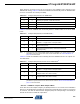
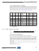
Table 14-8. Waveform Generation Mode Bit Description
Mode WGM2 WGM1 WGM0
Timer/Counter
Mode of
Operation TOP
Update of
OCRx at
TOV Flag
Set on
(1)(2)
0 0 0 0 Normal 0xFF Immediate MAX
10 0 1
PWM, Phase
Correct
0xFF TOP BOTTOM
2 0 1 0 CTC OCRA Immediate MAX
3 0 1 1 Fast PWM 0xFF BOTTOM MAX
4 1 0 0 Reserved – – –
51 0 1
PWM, Phase
Correct
OCRA TOP BOTTOM
6 1 1 0 Reserved – – –
7 1 1 1 Fast PWM OCRA BOTTOM TOP
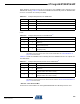
Bit 7 6 5 4 3 210
(0xB1)
FOC2A FOC2B – – WGM22 CS22 CS21 CS20 TCCR2B
Read/Write W W R R R/W R/W R/W R/W
Initial Value 0 0 0 0 0 0 0 0