
Datasheet

157
8011O–AVR–07/10
ATmega164P/324P/644P
Match on the following timer clock. Modifying the counter (TCNT2) while the counter is running,
introduces a risk of missing a Compare Match between TCNT2 and the OCR2x Registers.
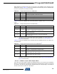
14.11.4 OCR2A – Output Compare Register A
The Output Compare Register A contains an 8-bit value that is continuously compared with the
counter value (TCNT2). A match can be used to generate an Output Compare interrupt, or to
generate a waveform output on the OC2A pin.
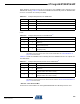
14.11.5 OCR2B – Output Compare Register B
The Output Compare Register B contains an 8-bit value that is continuously compared with the
counter value (TCNT2). A match can be used to generate an Output Compare interrupt, or to
generate a waveform output on the OC2B pin.
14.11.6 ASSR – Asynchronous Status Register
• Bit 6 – EXCLK: Enable External Clock Input
When EXCLK is written to one, and asynchronous clock is selected, the external clock input buf-
fer is enabled and an external clock can be input on Timer Oscillator 1 (TOSC1) pin instead of a
32 kHz crystal. Writing to EXCLK should be done before asynchronous operation is selected.
Note that the crystal Oscillator will only run when this bit is zero.
• Bit 5 – AS2: Asynchronous Timer/Counter2
When AS2 is written to zero, Timer/Counter2 is clocked from the I/O clock, clk
I/O
. When AS2 is
written to one, Timer/Counter2 is clocked from a crystal Oscillator connected to the Timer Oscil-
lator 1 (TOSC1) pin. When the value of AS2 is changed, the contents of TCNT2, OCR2A,
OCR2B, TCCR2A and TCCR2B might be corrupted.
• Bit 4 – TCN2UB: Timer/Counter2 Update Busy
When Timer/Counter2 operates asynchronously and TCNT2 is written, this bit becomes set.
When TCNT2 has been updated from the temporary storage register, this bit is cleared by hard-
ware. A logical zero in this bit indicates that TCNT2 is ready to be updated with a new value.
• Bit 3 – OCR2AUB: Output Compare Register2 Update Busy
When Timer/Counter2 operates asynchronously and OCR2A is written, this bit becomes set.
When OCR2A has been updated from the temporary storage register, this bit is cleared by hard-
ware. A logical zero in this bit indicates that OCR2A is ready to be updated with a new value.
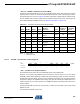
Bit 76543210
(0xB3) OCR2A[7:0] OCR2A
Read/Write R/W R/W R/W R/W R/W R/W R/W R/W
Initial Value00000000
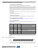
Bit 76543210
(0xB4) OCR2B[7:0] OCR2B
Read/Write R/W R/W R/W R/W R/W R/W R/W R/W
Initial Value00000000
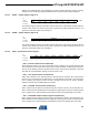
Bit 7 6 5 4 3 2 1 0
(0xB6) – EXCLK AS2 TCN2UB OCR2AUB OCR2BUB TCR2AUB TCR2BUB ASSR
Read/Write R R/W R/W R R R R R
Initial Value 0 0 0 0 0 0 0 0