
Datasheet

24
8011O–AVR–07/10
ATmega164P/324P/644P
While EEPE is set, any write to EEPMn will be ignored. During reset, the EEPMn bits will be
reset to 0b00 unless the EEPROM is busy programming.
• Bit 3 – EERIE: EEPROM Ready Interrupt Enable
Writing EERIE to one enables the EEPROM Ready Interrupt if the I-bit in SREG is set. Writing
EERIE to zero disables the interrupt. The EEPROM Ready interrupt generates a constant inter-
rupt when EEPE is cleared.
• Bit 2 – EEMPE: EEPROM Master Programming Enable
The EEMPE bit determines whether setting EEPE to one causes the EEPROM to be written.
When EEMPE is set, setting EEPE within four clock cycles will write data to the EEPROM at the
selected address If EEMPE is zero, setting EEPE will have no effect. When EEMPE has been
written to one by software, hardware clears the bit to zero after four clock cycles. See the
description of the EEPE bit for an EEPROM write procedure.
• Bit 1 – EEPE: EEPROM Programming Enable
The EEPROM Write Enable Signal EEPE is the write strobe to the EEPROM. When address
and data are correctly set up, the EEPE bit must be written to one to write the value into the
EEPROM. The EEMPE bit must be written to one before a logical one is written to EEPE, other-
wise no EEPROM write takes place. The following procedure should be followed when writing
the EEPROM (the order of steps 3 and 4 is not essential):
1. Wait until EEPE becomes zero.
2. Wait until SPMEN in SPMCSR becomes zero.
3. Write new EEPROM address to EEAR (optional).
4. Write new EEPROM data to EEDR (optional).
5. Write a logical one to the EEMPE bit while writing a zero to EEPE in EECR.
6. Within four clock cycles after setting EEMPE, write a logical one to EEPE.
The EEPROM can not be programmed during a CPU write to the Flash memory. The software
must check that the Flash programming is completed before initiating a new EEPROM write.
Step 2 is only relevant if the software contains a Boot Loader allowing the CPU to program the
Flash. If the Flash is never being updated by the CPU, step 2 can be omitted. See ”Memory Pro-
gramming” on page 293 for details about Boot programming.
Caution: An interrupt between step 5 and step 6 will make the write cycle fail, since the
EEPROM Master Write Enable will time-out. If an interrupt routine accessing the EEPROM is
interrupting another EEPROM access, the EEAR or EEDR Register will be modified, causing the
interrupted EEPROM access to fail. It is recommended to have the Global Interrupt Flag cleared
during all the steps to avoid these problems.
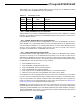
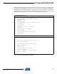
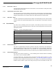
Table 5-1. EEPROM Mode Bits
EEPM1 EEPM0
Programming
Time Operation
0 0 3.4 ms Erase and Write in one operation (Atomic Operation)
0 1 1.8 ms Erase Only
1 0 1.8 ms Write Only
1 1 – Reserved for future use