
Datasheet


269
8011O–AVR–07/10
ATmega164P/324P/644P
22.4.2 IDCODE; 0x1
Optional JTAG instruction selecting the 32 bit ID-Register as Data Register. The ID-Register
consists of a version number, a device number and the manufacturer code chosen by JEDEC.
This is the default instruction after power-up.
The active states are:
• Capture-DR: Data in the IDCODE Register is sampled into the Boundary-scan Chain.
• Shift-DR: The IDCODE scan chain is shifted by the TCK input.
22.4.3 SAMPLE_PRELOAD; 0x2
Mandatory JTAG instruction for pre-loading the output latches and taking a snap-shot of the
input/output pins without affecting the system operation. However, the output latches are not
connected to the pins. The Boundary-scan Chain is selected as Data Register.
The active states are:
• Capture-DR: Data on the external pins are sampled into the Boundary-scan Chain.
• Shift-DR: The Boundary-scan Chain is shifted by the TCK input.
• Update-DR: Data from the Boundary-scan chain is applied to the output latches. However, the
output latches are not connected to the pins.
22.4.4 AVR_RESET; 0xC
The AVR specific public JTAG instruction for forcing the AVR device into the Reset mode or
releasing the JTAG reset source. The TAP controller is not reset by this instruction. The one bit
Reset Register is selected as Data Register. Note that the reset will be active as long as there is
a logic “one” in the Reset Chain. The output from this chain is not latched.
The active states are:
• Shift-DR: The Reset Register is shifted by the TCK input.
22.4.5 BYPASS; 0xF
Mandatory JTAG instruction selecting the Bypass Register for Data Register.
The active states are:
• Capture-DR: Loads a logic “0” into the Bypass Register.
• Shift-DR: The Bypass Register cell between TDI and TDO is shifted.
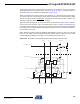
22.5 Boundary-scan Chain
The Boundary-scan chain has the capability of driving and observing the logic levels on the digi-
tal I/O pins, as well as the boundary between digital and analog logic for analog circuitry having
off-chip connection.
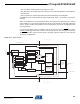
22.5.1 Scanning the Digital Port Pins
Figure 22-3 shows the Boundary-scan Cell for a bi-directional port pin. The pull-up function is
disabled during Boundary-scan when the JTAG IC contains EXTEST or SAMPLE_PRELOAD.
The cell consists of a bi-directional pin cell that combines the three signals Output Control -
OCxn, Output Data - ODxn, and Input Data - IDxn, into only a two-stage Shift Register. The port
and pin indexes are not used in the following description