
Datasheet

295
8011O–AVR–07/10
ATmega164P/324P/644P
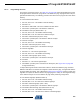
Note: 1. The SPIEN Fuse is not accessible in serial programming mode.
2. The default value of BOOTSZ1..0 results in maximum Boot Size. See Table 23-7 on page 288
for details.
3. See ”WDTCSR – Watchdog Timer Control Register” on page 59 for details.
4. Never ship a product with the OCDEN Fuse programmed regardless of the setting of Lock bits
and JTAGEN Fuse. A programmed OCDEN Fuse enables some parts of the clock system to
be running in all sleep modes. This may increase the power consumption.
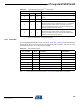
Note: 1. The default value of SUT1..0 results in maximum start-up time for the default clock source.
See ”System and Reset Characteristics” on page 331 for details.
2. The default setting of CKSEL3..0 results in internal RC Oscillator @ 8 MHz. See Table 6-1 on
page 30 for details.
3. The CKOUT Fuse allow the system clock to be output on PORTB1. See ”Clock Output Buffer”
on page 38 for details.
4. See ”System Clock Prescaler” on page 38 for details.
The status of the Fuse bits is not affected by Chip Erase. Note that the Fuse bits are locked if
Lock bit1 (LB1) is programmed. Program the Fuse bits before programming the Lock bits.
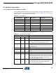
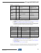
Table 24-4. Fuse High Byte
Fuse High Byte Bit No Description Default Value
OCDEN
(4)
7Enable OCD
1 (unprogrammed, OCD
disabled)
JTAGEN 6 Enable JTAG 0 (programmed, JTAG enabled)
SPIEN
(1)
5
Enable Serial Program and Data
Downloading
0 (programmed, SPI prog.
enabled)
WDTON
(3)
4 Watchdog Timer always on 1 (unprogrammed)
EESAVE 3
EEPROM memory is preserved
through the Chip Erase
1 (unprogrammed, EEPROM
not preserved)
BOOTSZ1 2
Select Boot Size (see Table 24-9 for
details)
0 (programmed)
(2)
BOOTSZ0 1
Select Boot Size (see Table 24-9 for
details)
0 (programmed)
(2)
BOOTRST 0 Select Reset Vector 1 (unprogrammed)
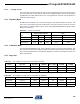
Table 24-5. Fuse Low Byte
Fuse Low Byte Bit No Description Default Value
CKDIV8
(4)
7 Divide clock by 8 0 (programmed)
CKOUT
(3)
6 Clock output 1 (unprogrammed)
SUT1 5 Select start-up time 1 (unprogrammed)
(1)
SUT0 4 Select start-up time 0 (programmed)
(1)
CKSEL3 3 Select Clock source 0 (programmed)
(2)
CKSEL2 2 Select Clock source 0 (programmed)
(2)
CKSEL1 1 Select Clock source 1 (unprogrammed)
(2)
CKSEL0 0 Select Clock source 0 (programmed)
(2)