8/16-bit Atmel AVR XMEGA Microcontrollers ATxmega32E5 / ATxmega16E5 / ATxmega8E5 DATASHEET Features High-performance, low-power Atmel® AVR® XMEGA® 8/16-bit Microcontroller Nonvolatile program and data memories 8K –32KB of in-system self-programmable flash 2K – 4KB boot section 512Bytes – 1KB EEPROM 1K – 4KB internal SRAM Peripheral features Four-channel enhanced DMA controller with 8/16-bit address match Eight-channel event system Asynchronous a
1.
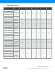
Package(1)(2)(3) Ordering Code ATxmega32E5-AN ATxmega32E5ANR ATxmega32E5-MN (4) ATxmega32E5-M4N ATxmega32E5-M4NR Notes: 1. 2. 3. 4. EEPROM [Bytes] SRAM [Bytes] Speed [MHz] Power supply [V] Temp. [°C] 32K + 4K 1K 4K 32 1.6 – 3.6 -40 – 105 32A (7x7mm TQFP) (4) ATxmega32E5-MNR Flash [Bytes] (4) 32Z (5x5mm VQFN) 32MA (4x4mm UQFN) This device can also be supplied in wafer form. Please contact your local Atmel sales office for detailed ordering information.
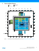
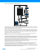
Pinout and Block Diagram Power Programming, debug, test Ground External clock / Crystal pins Digital function General Purpose I/O PD1 PD2 PD3 26 25 PA7 29 27 PA6 30 PD0 PA5 31 28 AVCC 32 Analog function / Oscillators 24 PD4 23 PD5 22 PD6 21 PD7 20 PR0 19 PR1 18 GND 17 VCC XCL USART0 2 TC5 PA4 AREF 1 ADC Port D GND EVENT ROUTING NETWORK DATA BUS PA3 3 AREF 4 TEMPREF Watchdog Oscillator Reset Controller Real Time Counter VREF Sleep Controller OSC/CLK Cont
4. Overview The Atmel AVR XMEGA is a family of low power, high performance, and peripheral rich 8/16-bit microcontrollers based on the AVR enhanced RISC architecture. By executing instructions in a single clock cycle, the AVR XMEGA devices achieve CPU throughput approaching one million instructions per second (MIPS) per megahertz, allowing the system designer to optimize power consumption versus processing speed. The AVR CPU combines a rich instruction set with 32 general purpose working registers.
5. Resources A comprehensive set of development tools, application notes and datasheets are available for download on http://www.atmel.com/avr. 5.1 Recommended Reading XMEGA E Manual XMEGA Application Notes This device data sheet only contains part specific information with a short description of each peripheral and module. The XMEGA E Manual describes the modules and peripherals in depth. The XMEGA application notes contain example code and show applied use of the modules and peripherals.
. CPU 7.1 Features 8/16-bit, high-performance Atmel AVR RISC CPU 142 instructions Hardware multiplier 32x8-bit registers directly connected to the ALU Stack in RAM Stack pointer accessible in I/O memory space Direct addressing of up to 16MB of program memory and 16MB of data memory True 16/24-bit access to 16/24-bit I/O registers Efficient support for 8-, 16-, and 32-bit arithmetic Configuration change protection of system-critical features 7.
Figure 7-1. Block Diagram of the AVR CPU Architecture The arithmetic logic unit (ALU) supports arithmetic and logic operations between registers or between a constant and a register. Single-register operations can also be executed in the ALU. After an arithmetic operation, the status register is updated to reflect information about the result of the operation. The ALU is directly connected to the fast-access register file.
7.4 ALU - Arithmetic Logic Unit The arithmetic logic unit (ALU) supports arithmetic and logic operations between registers or between a constant and a register. Single-register operations can also be executed. The ALU operates in direct connection with all 32 general purpose registers. In a single clock cycle, arithmetic operations between general purpose registers or between a register and an immediate are executed and the result is stored in the register file.
after reset, and the initial value is the highest address of the internal SRAM. If the SP is changed, it must be set to point above address 0x2000, and it must be defined before any subroutine calls are executed or before interrupts are enabled. During interrupts or subroutine calls, the return address is automatically pushed on the stack. The return address can be two or three bytes, depending on program memory size of the device.
8. Memories 8.
All AVR CPU instructions are 16 or 32 bits wide, and each flash location is 16 bits wide. The flash memory is organized in two main sections, the application section and the boot loader section. The sizes of the different sections are fixed, but device-dependent. These two sections have separate lock bits, and can have different levels of protection.
the corresponding peripheral registers from software. For details on calibration conditions, refer to “Electrical Characteristics” on page 71. The production signature row also contains an ID that identifies each microcontroller device type and a serial number for each manufactured device. The serial number consists of the production lot number, wafer number, and wafer coordinates for the device. The device ID for the available devices is shown in Table 8-1.
8.5 Data Memory The data memory contains the I/O memory, internal SRAM and EEPROM. The data memory is organized as one continuous memory section, see Table 8-2 on page 15. To simplify development, I/O Memory, EEPROM and SRAM will always have the same start addresses for all XMEGA devices. Figure 8-2. Data Memory Map (hexadecimal value) Byte Address ATxmega32E5 0 FFF Byte Address I/O Registers (4K) 1000 EEPROM (1K) 13FF ATxmega16E5 0 FFF 1000 11FF RESERVED 2000 2FFF 8.
8.10 Device ID and Revision Each device has a three-byte device ID. This ID identifies Atmel as the manufacturer of the device and the device type. A separate register contains the revision number of the device. 8.11 I/O Memory Protection Some features in the device are regarded as critical for safety in some applications. Due to this, it is possible to lock the I/O register related to the clock system, the event system, and the waveform extensions.
9. EDMA – Enhanced DMA Controller 9.
The EDMA controller supports extended features such as double buffering, data match for peripherals and data search for SRAM or EEPROM. The EDMA controller supports two types of channel. Each channel type can be selected individually.
10. Event System 10.
Figure 10-1. Event System Overview and Connected Peripherals CPU / Software EDMA Controller Event Routing Network ADC Event System Controller AC DAC clkPER Prescaler Real Time Counter Timer / Counters XMEGA Custom Logic IRCOM Port Pins The event routing network consists of eight software-configurable multiplexers that control how events are routed and used. These are called event channels, and allow up to eight parallel event configurations and routing.
11. System Clock and Clock options 11.1 Features Fast start-up time Safe run-time clock switching Internal Oscillators: 32MHz run-time calibrated and tuneable oscillator 8MHz calibrated oscillator with 2MHz output option and fast start-up 32.768kHz calibrated oscillator 32kHz Ultra Low Power (ULP) oscillator with 1kHz output External clock options 0.
Figure 11-1. The Clock System, Clock Sources, and Clock Distribution Real Time Counter Peripherals RAM Non-Volatile Memory AVR CPU clkPER clkCPU clkPER2 clkPER4 clk RTC Brown-out Detector System Clock Prescalers Watchdog Timer clkSYS System Clock Multiplexer (SCLKSEL) DIV32 DIV32 DIV32 RTCSRC PLL 11.3 XTAL2 0.4 – 16 MHz XTAL XTAL1 32.768 kHz TOSC TOSC2 32.768 kHz Int. OSC TOSC1 32 kHz Int. ULP 32 MHz Int. Osc 8 MHz Int.
11.3.2 32.768kHz Calibrated Internal Oscillator This oscillator provides an approximate 32.768kHz clock. It is calibrated during production to provide a default frequency close to its nominal frequency. The calibration register can also be written from software for run-time calibration of the oscillator frequency. The oscillator employs a built-in prescaler, which provides both a 32.768kHz output and a 1.024kHz output. 11.3.3 32.768kHz Crystal Oscillator A 32.
12. Power Management and Sleep Modes 12.1 Features Power management for adjusting power consumption and functions Five sleep modes Idle Power down Power save Standby Extended standby Power reduction register to disable clock and turn off unused peripherals in active and idle modes 12.2 Overview Various sleep modes and clock gating are provided in order to tailor power consumption to application requirements.
12.3.3 Power-save Mode Power-save mode is identical to power down, with one exception. If the real-time counter (RTC) is enabled, it will keep running during sleep, and the device can also wake up from either an RTC overflow or compare match interrupt. Low power mode option of 8MHz internal oscillator enables instant oscillator wake-up time. This reduces the MCU wake-up time or enables the MCU wake-up from UART bus. 12.3.
13. System Control and Reset 13.1 Features Reset the microcontroller and set it to initial state when a reset source goes active Multiple reset sources that cover different situations Power-on reset External reset Watchdog reset Brownout reset PDI reset Software reset Asynchronous operation No running system clock in the device is required for reset Reset status register for reading the reset source from the application code 13.
13.4.2 Brownout Detection The on-chip brownout detection (BOD) circuit monitors the VCC level during operation by comparing it to a fixed, programmable level that is selected by the BODLEVEL fuses. If disabled, BOD is forced on at the lowest level during chip erase and when the PDI is enabled. 13.4.3 External Reset The external reset circuit is connected to the external RESET pin.
14. WDT – Watchdog Timer 14.1 Features Issues a device reset if the timer is not reset before its timeout period Asynchronous operation from dedicated oscillator 1kHz output of the 32kHz ultra low power oscillator 11 selectable timeout periods, from 8ms to 8s Two operation modes: Normal mode Window mode Configuration lock to prevent unwanted changes 14.2 Overview The watchdog timer (WDT) is a system function for monitoring correct program operation.
15. Interrupts and Programmable Multilevel Interrupt Controller 15.
Program address (base address) Source Interrupt description 0x0024 TCC5_INT_base Timer/counter 5 on port C interrupt base 0x002C SPIC_INT_vect SPI on port C interrupt vector 0x002E USARTC0_INT_base USART 0 on port C interrupt base 0x0034 NVM_INT_base Non-Volatile Memory interrupt base 0x0038 XCL_INT_base XCL (programmable logic) module interrupt base 0x003C PORTA_INT_vect Port A interrupt vector 0x003E ACA_INT_base Analog comparator on Port A interrupt base 0x0044 ADCA_INT_base Ana
16. I/O Ports 16.
16.3 Output Driver All port pins (Pxn) have programmable output configuration. The port pins also have configurable slew rate limitation to reduce electromagnetic emission. 16.3.1 Push-pull Figure 16-1. I/O Configuration - Totem-pole DIRxn OUTxn Pxn INxn 16.3.2 Pull-down Figure 16-2. I/O Configuration - Totem-pole with Pull-down (on input) DIRxn OUTxn Pxn INxn 16.3.3 Pull-up Figure 16-3.
16.3.4 Bus-keeper The bus-keeper’s weak output produces the same logical level as the last output level. It acts as a pull-up if the last level was ‘1’, and pull-down if the last level was ‘0’. Figure 16-4. I/O Configuration - Totem-pole with Bus-keeper DIRxn OUTxn Pxn INxn 16.3.5 Others Figure 16-5. Output Configuration - Wired-OR with Optional Pull-down OUTxn Pxn INxn Figure 16-6.
16.4 Input Sensing Input sensing is synchronous or asynchronous depending on the enabled clock for the ports, and the configuration is shown in Figure 16-7. Figure 16-7. Input Sensing System Overview Asynchronous sensing EDGE DETECT Interrupt Control IRQ Synchronous sensing Pxn Synchronizer INn D Q D R Q EDGE DETECT Synchronous Events R INVERTED I/O Asynchronous Events When a pin is configured with inverted I/O, the pin value is inverted before the input sensing. 16.
17. Timer Counter Type 4 and 5 17.
There are two differences between timer/counter type 4 and type 5. Timer/counter 4 has four CC channels, and timer/counter 5 has two CC channels. Both timer/counter 4 and 5 can be set in 8-bit mode, allowing the application to double the number of compare and capture channels that then get 8-bit resolution. Some timer/counters have extensions that enable more specialized waveform generation.
18. WeX – Waveform Extension 18.
The output override disable unit can disable the waveform output on selectable port pins to optimize the pins usage. This is to free the pins for other functional use, when the application does not need the waveform output spread across all the port pins as they can be selected by the OTMX configurations. The waveform extension is available for TCC4 and TCC5. The notation of this is WEXC.
19. Hi-Res – High Resolution Extension 19.1 Features Increases waveform generator resolution up to 8x (three bits) Supports frequency, single-slope PWM, and dual-slope PWM generation Supports the WeX when this is used for the same timer/counter 19.2 Overview The high-resolution (hi-res) extension can be used to increase the resolution of the waveform generation output from a timer/counter by four or eight.
20. Fault Extension 20.
21. RTC – 16-bit Real-Time Counter 21.1 Features 16-bit resolution Selectable clock source 32.768kHz external crystal External clock 32.768kHz internal oscillator 32kHz internal ULP oscillator Programmable 10-bit clock prescaling One compare register One period register Clear counter on period overflow Optional interrupt/event on overflow and compare match Correction for external crystal oscillator frequency error down to ±0.5ppm accuracy 21.
Figure 21-1. Real-time Counter Overview External Clock TOSC1 TOSC2 32.768 kHz Crystal Osc 32.768 kHz Int. Osc DIV32 DIV32 32 kHz int ULP (DIV32) RTCSRC CALIB clkRTC PER = Correction Counter Hold Count 10-bit prescaler TOP/ Overflow CNT = ”match”/ Compare COMP The RTC also supports correction when operated using external 32.768 kHz crystal oscillator. An externally calibrated value will be used for correction.
22. TWI – Two-Wire Interface 22.
It is possible to disable the TWI drivers in the device, and enable a four-wire digital interface for connecting to an external TWI bus driver. This can be used for applications where the device operates from a different VCC voltage than used by the TWI bus. It is also possible to enable the bridge mode. In this mode, the slave I/O pins are selected from an alternative port, enabling independent and simultaneous master and slave operation. PORTC has one TWI. Notation of this peripheral is TWIC.
23. SPI – Serial Peripheral Interface 23.1 Features One SPI peripheral Full-duplex, three-wire synchronous data transfer Master or slave operation lsb first or msb first data transfer Eight programmable bit rates Interrupt flag at the end of transmission Write collision flag to indicate data collision Wake up from idle sleep mode Double speed master mode 23.
24. USART 24.
The clock generator includes a fractional baud rate generator that is able to generate a wide range of USART baud rates from any system clock frequencies. This removes the need to use an external crystal oscillator with a specific frequency to achieve a required baud rate. It also supports external clock input in synchronous slave operation. An IRCOM module can be enabled for one USART to support IrDA 1.4 physical compliant pulse modulation and demodulation for baud rates up to 115.2Kbps.
25. IRCOM – IR Communication Module 25.1 Features Pulse modulation/demodulation for infrared communication IrDA compatible for baud rates up to 115.2Kbps Selectable pulse modulation scheme 3/16 of the baud rate period Fixed pulse period, 8-bit programmable Pulse modulation disabled Built-in filtering Can be connected to and used by any USART 25.2 Overview Atmel AVR XMEGA devices contain an infrared communication module (IRCOM) that is IrDA compatible for baud rates up to 115.2Kbps.
26. XCL – XMEGA Custom Logic Module 26.
The LUT works in all sleep modes. Combined with event system and one I/O pin, the LUT can wake-up the system if, and only if, condition on up to three input pins is true. A block diagram of the programmable logic unit with extensions and closely related peripheral modules (in grey) is shown in Figure 26-1. Figure 26-1.
27. CRC – Cyclic Redundancy Check Generator 27.
28. ADC – 12-bit Analog to Digital Converter 28.1 Features 12-bit resolution Up to 300 thousand samples per second Down to 2.3μs conversion time with 8-bit resolution Down to 3.
Figure 28-1. ADC Overview VIN S&H ADC ADC0 ADC1 • • • ADC14 ADC15 2x VOUT DAC 2 bits Stage 1 VINP 2 Internal Signals ADC0 • • • ADC7 Σ ½x - 64x CMP Stage 2 clkADC Digital Correction Logic VINN Internal 1.00V Internal AVCC/1.6 Internal AVCC/2 AREFA AREFD ADC < > 2 Gain & Offset Error Correction Threshold (Int. Req.) RES Averaging Reference Voltage The ADC may be configured for 8- or 12-bit result, reducing the propagation delay from 3.35µs for 12-bit to 2.3µs for 8-bit result.
29. DAC – Digital to Analog Converter 29.
30. AC – Analog Comparator 30.
Figure 30-1. Analog Comparator Overview Pin Input AC0OUT Pin Input Hysteresis DAC Enable Voltage Scaler ACnMUXCTRL ACnCTRL Interrupt Mode WINCTRL Enable Bandgap Interrupt Sensititivity Control & Window Function Interrupts Events Hysteresis Pin Input AC1OUT Pin Input The window function is realized by connecting the external inputs of the two analog comparators in a pair as shown in Figure 30-2. Figure 30-2.
31. Programming and Debugging 31.
32. Pinout and Pin Functions The device pinout is shown in “Pinout and Block Diagram” on page 4. In addition to general purpose I/O functionality, each pin can have several alternate functions. This will depend on which peripheral is enabled and connected to the actual pin. Only one of the pin functions can be used at time. 32.1 Alternate Pin Function Description The tables below show the notation for all pin functions available and describe its function. 32.1.
XCKn Transfer Clock for USART n RXDn Receiver Data for USART n TXDn Transmitter Data for USART n SS Slave Select for SPI MOSI Master Out Slave In for SPI MISO Master In Slave Out for SPI SCK Serial Clock for SPI 32.1.6 Oscillators, Clock, and Event TOSCn Timer Oscillator pin n XTALn Input/Output for Oscillator pin n CLKOUT Peripheral Clock Output EVOUT Event Channel Output RTCOUT RTC Clock Source Output 32.1.
32.2 Alternate Pin Functions The tables below show the primary/default function for each pin on a port in the first column, the pin number in the second column, and then all alternate pin functions in the remaining columns. The head row shows what peripheral that enable and use the alternate pin functions. For better flexibility, some alternate functions also have selectable pin locations for their functions, this is noted under the first table where this apply. Table 32-1.
Table 32-4. PORT R – Alternate Functions PORT R Pin # XTAL TOSC PR0 20 XTAL2 TOSC2 PR1 19 XTAL1 TOSC1 EXTCLK CLOCKOUT EVENTOUT RTCOUT AC OUT CLKOUT EVOUT RTCOUT AC1 OUT EXTCLK AC0 OUT Table 32-5.
33. Peripheral Module Address Map The address maps show the base address for each peripheral and module in XMEGA E5. For complete register description and summary for each peripheral module, refer to the XMEGA E Manual. Table 33-1.
Base Address Name Description 0x07E0 PORTR Port R 0x0800 TCC4 Timer/Counter 4 on port C 0x0840 TCC5 Timer/Counter 5 on port C 0x0880 FAULTC4 Fault Extension on TCC4 0x0890 FAULTC5 Fault Extensionon TCC5 0x08A0 WEXC Waveform Extension on port C 0x08B0 HIRESC High Resolution Extension on port C 0x08C0 USARTC0 USART 0 on port C 0x08E0 SPIC Serial Peripheral Interface on port C 0x08F8 IRCOM Infrared Communication Module 0x0940 TCD5 Timer/Counter 5 on port D 0x09C0 USARTD0 U
34.
Mnemonics Operands Description Operation Flags #Clocks ICALL Indirect Call to (Z) PC(15:0) PC(21:16) Z, 0 None 2 / 3(1) EICALL Extended Indirect Call to (Z) PC(15:0) PC(21:16) Z, EIND None 3(1) call Subroutine PC k None 3 / 4(1) RET Subroutine Return PC STACK None 4 / 5(1) RETI Interrupt Return PC STACK I 4 / 5(1) if (Rd = Rr) PC PC + 2 or 3 None 1/2/3 CALL k CPSE Rd,Rr Compare, Skip if Equal CP Rd,Rr Compare CPC Rd,Rr Compare with Carry
Mnemonics Operands Description LDS Rd, k Load Direct from data space Rd (k) None 2(1)(2) LD Rd, X Load Indirect Rd (X) None 1(1)(2) LD Rd, X+ Load Indirect and Post-Increment Rd X (X) X+1 None 1(1)(2) LD Rd, -X Load Indirect and Pre-Decrement X X - 1, Rd (X) X-1 (X) None 2(1)(2) LD Rd, Y Load Indirect Rd (Y) (Y) None 1(1)(2) LD Rd, Y+ Load Indirect and Post-Increment Rd Y (Y) Y+1 None 1(1)(2) LD Rd, -Y Load Indirect and Pre-Decreme
Mnemonics Operands Description Operation SPM Z+ Store Program Memory and Post-Increment by 2 IN Rd, A In From I/O Location OUT A, Rr Out To I/O Location PUSH Rr Push Register on Stack POP Rd XCH Flags #Clocks (RAMPZ:Z) Z R1:R0, Z+2 None - Rd I/O(A) None 1 I/O(A) Rr None 1 STACK Rr None 1(1) Pop Register from Stack Rd STACK None 2(1) Z, Rd Exchange RAM location Temp Rd (Z) Rd, (Z), Temp None 2 LAS Z, Rd Load and Set RAM location Temp
Mnemonics Operands Description Operation Flags #Clocks I 0 I 1 Set Signed Test Flag S 1 S 1 CLS Clear Signed Test Flag S 0 S 1 SEV Set Two’s Complement Overflow V 1 V 1 CLV Clear Two’s Complement Overflow V 0 V 1 SET Set T in SREG T 1 T 1 CLT Clear T in SREG T 0 T 1 SEH Set Half Carry Flag in SREG H 1 H 1 CLH Clear Half Carry Flag in SREG H 0 H 1 None 1 None 1 CLI Global Interrupt Disable SES MCU control instructions
35. Packaging Information 35.
35.
35.
36. Electrical Characteristics All typical values are measured at T = 25°C unless other temperature condition is given. All minimum and maximum values are valid across operating temperature and voltage unless other conditions are given. 36.1 Absolute Maximum Ratings Symbol 36.2 Parameter Min. Typ. Max. Units VCC Power supply voltage -0.3 4 V IVCC Current into a VCC pin 200 IGND Current out of a Gnd pin 200 VPIN Pin voltage with respect to Gnd and VCC -0.5 VCC+0.
Figure 36-1. Maximum Frequency vs. VCC MHz 32 Safe Operating Area 12 1.6 1.8 2.7 3.
36.3 Current Consumption Table 36-3. Current Consumption for Active Mode and Sleep Modes Symbol Parameter Condition Min. 32kHz, Ext. Clk Active power consumption (1) 1MHz, Ext. Clk 2MHz, Ext. Clk 32MHz, Ext. Clk 32kHz, Ext. Clk Idle power consumption (1) 1MHz, Ext. Clk 2MHz, Ext. Clk 32MHz, Ext. Clk All disabled, T = 85°C 20 VCC = 3.0V 35 VCC = 1.8V 155 VCC = 3.0V 290 VCC = 1.8V 300 400 VCC = 3.0V 0.6 1.2 VCC = 3.0V 7 10 VCC = 1.8V 7 VCC = 3.0V 12 VCC = 1.8V 55 VCC = 3.
Table 36-4. Current Consumption for Modules and Peripherals Symbol Parameter Condition(1) Min. Internal ULP oscillator 100 32.768kHz int. oscillator 27 8MHz int. oscillator 32MHz int. oscillator PLL Normal power mode 65 Low power mode 45 BOD Max. Units nA 275 DFLL enabled with 32.768kHz int. osc. as reference 20x multiplication factor, 400 230 32MHz int. osc. DIV4 as reference Watchdog timer µA 0.3 Continuous mode 245 Sampled mode 0.4 Internal 1.
36.4 Wake-up Time from Sleep Modes Table 36-5. Device Wake-up Time from Sleep Modes with Various System Clock Sources Symbol Parameter Wake-up time from idle, standby, and extended standby mode Wake-up time from power save mode twakeup Wake-up time from power down mode Notes: 1. Condition Min. Typ.(1) External 2MHz clock 0.2 32kHz internal oscillator 120 8MHz internal oscillator 0.5 32MHz internal oscillator 0.2 External 2MHz clock 4.
36.5 I/O Pin Characteristics The I/O pins complies with the JEDEC LVTTL and LVCMOS specification and the high- and low-level input and output voltage limits reflect or exceed this specification. Table 36-6. I/O Pin Characteristics Symbol IOH (1)/ Parameter Condition I/O pin source/sink current IOL (2) Min. Typ. Max. Units -15 15 mA VIH High level input voltage, except XTAL1 and RESET pin VCC = 2.4 - 3.6V 0.7*VCC VCC+0.5 VCC = 1.6 - 2.4V 0.8*VCC VCC+0.
Symbol Parameter Vin Input range Vin Conversion range Vin Conversion range Table 36-8. Symbol ClkADC Condition Min. VREF Differential mode, Vinp - Vinn -0.95*VREF 0.95*VREF Single ended unsigned mode, Vinp -0.05*VREF 0.95*VREF Condition Min. Maximum is 1/4 of Peripheral clock frequency 100 Table 36-9. Symbol RES Parameter ADC Clock frequency Sample rate Sample rate Typ. Max.
Symbol Condition(2) Parameter Differential mode DNL(1) Differential non-linearity Single ended unsigned mode Offset Error Gain Error Differential mode Min. 1 16ksps, VREF = 1V 2 300ksps, VREF = 3V 1 300ksps, VREF = 1V 2 16ksps, VREF = 3.0V 1 1.5 16ksps, VREF = 1.0V 2 3 lsb mV Temperature drift 0.01 mV/K Operating voltage drift 0.25 mV/V External reference -5 AVCC/1.6 -5 AVCC/2.0 -6 Bandgap ±10 Differential mode mV 0.
Symbol Parameter Condition Typ. 0.5x gain -1 1x gain -1 8x gain -1 64x gain -1.5 0.5x gain 10 Offset error, 1x gain 5 input referred 8x gain 5 64x gain 5 Gain error 36.7 Min. Max. Units % mV DAC Characteristics Table 36-11.
Table 36-13. Accuracy Characteristics Symbol RES Parameter Condition Min. Typ. Input Resolution VREF= Ext 1.0V INL (1) Integral non-linearity VREF=AVCC VREF=INT1V VREF=Ext 1.0V DNL (1) Differential non-linearity VREF=AVCC VREF=INT1V Gain error Max. Units 12 Bits VCC = 1.6V ±2.0 ±3 VCC = 3.6V ±1.5 ±2.5 VCC = 1.6V ±2.0 ±4 VCC = 3.6V ±1.5 ±4 VCC = 1.6V ±5.0 VCC = 3.6V ±5.0 VCC = 1.6V ±1.5 3 VCC = 3.6V ±0.6 1.5 VCC = 1.6V ±1.0 3.5 VCC = 3.6V ±0.6 1.5 VCC = 1.
Symbol Parameter Condition Min. 64-Level Voltage Scaler Integral nonlinearity (INL) Current source accuracy after calibration 36.9 Typ. Max. Units 0.3 0.5 lsb 5 % Current source calibration range Single mode 4 6 Current source calibration range Double mode 8 12 µA Bandgap and Internal 1.0V Reference Characteristics Table 36-15. Bandgap and Internal 1.0V Reference Characteristics Symbol Parameter Condition Min. As reference for ADC Startup time BANDGAP INT1V 36.9.1 Typ. Max.
36.10 External Reset Characteristics Table 36-16. External Reset Characteristics Symbol tEXT Parameter Minimum reset pulse width Reset threshold voltage (VIH) VRST Reset threshold voltage (VIL) RRST Condition Min. Typ. 90 1000 VCC = 2.7 - 3.6V 0.6*VCC VCC = 1.6 - 2.7V 0.6*VCC Max. ns VCC = 2.7 - 3.6V 0.5*VCC VCC = 1.6 - 2.7V 0.4*VCC Reset pin Pull-up Resistor Units V 25 k 36.11 Power-on Reset Characteristics Table 36-17.
Table 36-19. Programming Time Parameter Condition Chip Erase Flash EEPROM Notes: 1. 2. Min. Typ.(1) 32KB Flash, EEPROM(2) 50 (2) 45 16KB Flash, EEPROM 8KB Flash, EEPROM(2) 42 Page erase 4 Page write 4 Atomic page erase and write 8 Page erase 4 Page write 4 Atomic page erase and write 8 Max. Units ms Programming is timed from the 2MHz output of 8MHz internal oscillator. EEPROM is not erased if the EESAVE fuse is programmed.
36.13 Clock and Oscillator Characteristics 36.13.1 Calibrated 32.768kHz Internal Oscillator Characteristics Table 36-20. 32.768kHz Internal Oscillator Characteristics Symbol Parameter Condition Min. Frequency Factory calibration accuracy Typ. Max. 32.768 T = 25°C, VCC = 3.0V User calibration accuracy Units kHz -0.5 0.5 -0.5 0.5 % 36.13.2 Calibrated 8MHz Internal Oscillator Characteristics Table 36-21. 8MHz Internal Oscillator Characteristics Symbol Parameter Condition Min.
36.13.5 Internal Phase Locked Loop (PLL) Characteristics Table 36-24. Internal PLL Characteristics Symbol fIN Condition Input frequency Output frequency (1) fOUT Note: Parameter 1. Min. Typ. Max. Output frequency must be within fOUT 0.4 64 VCC= 1.6 - 1.8V 20 48 VCC= 2.7 - 3.6V 20 128 Start-up time 25 Re-lock time 25 Units MHz µs The maximum output frequency vs. supply voltage is linear between 1.8V and 2.7V, and can never be higher than four times the maximum CPU frequency. 36.13.
Table 36-26. External Clock with Prescaler (1) for System Clock Symbol Parameter Condition Clock Frequency (2) 1/tCK tCK Clock Period tCH Clock High Time tCL Clock Low Time tCR Rise Time (for maximum frequency) tCF Fall Time (for maximum frequency) tCK Notes: Min. Typ. VCC = 1.6 - 1.8V 0 90 VCC = 2.7 - 3.6V 0 142 VCC = 1.6 - 1.8V 11 VCC = 2.7 - 3.6V 7 VCC = 1.6 - 1.8V 4.5 VCC = 2.7 - 3.6V 2.4 VCC = 1.6 - 1.8V 4.5 VCC = 2.7 - 3.6V 2.4 Units MHz ns VCC = 1.6 - 1.8V 1.
Symbol Parameter Frequency error Condition XOSCPWR=0 Min. FRQRANGE=0 <0.1 FRQRANGE=1 <0.05 FRQRANGE=2 or 3 <0.005 XOSCPWR=1 Duty cycle XOSCPWR=0 Max. <0.005 FRQRANGE=0 40 FRQRANGE=1 42 FRQRANGE=2 or 3 45 XOSCPWR=1 XOSCPWR=0, FRQRANGE=0 Typ. Units % 48 0.
Symbol Parameter Condition Min. Typ. CXTAL1 Parasitic capacitance XTAL1 pin 5.4 CXTAL2 Parasitic capacitance XTAL2 pin 7.1 CLOAD Parasitic capacitance load 3.07 Note: 1. Max. Units pF Numbers for negative impedance are not tested in production but guaranteed from design and characterization. 36.13.8 External 32.768kHz Crystal Oscillator and TOSC Characteristics Table 36-28. External 32.
36.14 SPI Characteristics Figure 36-5. SPI Timing Requirements in Master Mode SS tSCKR tMOS tSCKF SCK (CPOL = 0) tSCKW SCK (CPOL = 1) tSCKW tMIS MISO (Data Input) tMIH tSCK MSB LSB tMOH tMOH MOSI (Data Output) MSB LSB Figure 36-6.
Table 36-29. SPI Timing Characteristics and Requirements Symbol Parameter Condition Min. Typ. Max. tSCK SCK period Master tSCKW SCK high/low width Master 0.5×SCK tSCKR SCK rise time Master 2.7 tSCKF SCK fall time Master 2.7 tMIS MISO setup to SCK Master 10 tMIH MISO hold after SCK Master 10 tMOS MOSI setup SCK Master 0.5×SCK tMOH MOSI hold after SCK Master 1.
36.15 Two-Wire Interface Characteristics Table 36-6 on page 76 describes the requirements for devices connected to the two-wire interface (TWI) Bus. The Atmel AVR XMEGA TWI meets or exceeds these requirements under the noted conditions. Timing symbols refer to Figure 367. Figure 36-7. Two-wire Interface Bus Timing tof tHIGH tLOW tr SCL tSU;STA tHD;DAT tSU;STO tSU;DAT tHD;STA SDA tBUF Table 36-30. Two-wire Interface Characteristics Symbol Parameter Condition Min. Typ. Max.
Symbol tLOW Low period of SCL Clock tHIGH High period of SCL Clock Set-up time for a repeated START condition tSU;STA tHD;DAT Data hold time tSU;DAT Data setup time tSU;STO Setup time for STOP condition Bus free time between a STOP and START condition tBUF Notes: Parameter 1. 2. 3. Condition Min. fSCL ≤ 100kHz 4.7 fSCL ≤ 400kHz 1.3 fSCL ≤ 1MHz 0.5 fSCL ≤ 100kHz 4 fSCL ≤ 400kHz 0.6 fSCL ≤ 1MHz 0.26 fSCL ≤ 100kHz 4.7 fSCL ≤ 400kHz 0.6 fSCL ≤ 1MHz 0.26 Typ. Max.
37. Typical Characteristics 37.1 Current Consumption 37.1.1 Active Mode Supply Current Figure 37-1. Active Mode Supply Current vs. Frequency fSYS = 0 – 1MHz external clock, T = 25°C V_CC_ 0.35 1.6 1.8 ICC [mA] 0.30 2.2 0.25 2.7 0.20 3 3.6 0.15 0.10 0.05 0.00 0.0 0.2 0.4 0.6 0.8 1.0 Frequency [MHz] Figure 37-2. Active Mode Supply Current vs. Frequency fSYS = 0 – 32MHz external clock, T = 25°C V_CC_ 9 1.8 8 2.2 7 2.7 6 ICC [mA] 1.6 3 5 3.
Figure 37-3. Active Mode Supply Current vs. VCC fSYS = 32.768kHz internal oscillator Temperature 38.0 -40 37.0 25 36.0 85 35.0 105 ICC [uA] 34.0 33.0 32.0 31.0 30.0 29.0 28.0 27.0 1.6 1.8 2.0 2.2 2.4 2.6 2.8 3.0 3.2 3.4 3.6 Vcc [V] Figure 37-4. Active Mode Supply Current vs. VCC fSYS = 1MHz external clock Temperature 0.35 -40 25 85 0.30 ICC [mA] 105 0.25 0.20 0.15 0.10 1.6 1.8 2.0 2.2 2.4 2.6 2.8 3.0 3.2 3.4 3.
Figure 37-5. Active Mode Supply Current vs. VCC fSYS = 8MHz internal oscillator prescaled to 2MHz Temperature 0.8 -40 25 0.7 85 105 ICC [mA] 0.6 0.5 0.4 0.3 0.2 1.6 1.8 2.0 2.2 2.4 2.6 2.8 3.0 3.2 3.4 3.6 Vcc [V] Figure 37-6. Active Mode Supply Current vs. VCC fSYS = 8MHz internal oscillator Temperature 2.5 -40 25 85 ICC [mA] 2.0 105 1.5 1.0 0.5 1.6 1.8 2.0 2.2 2.4 2.6 2.8 3.0 3.2 3.4 3.
Figure 37-7. Active mode Supply Current vs. VCC fSYS = 32MHz internal oscillator prescaled to 8MHz Temperature 3.0 -40 25 85 2.5 ICC [mA] 105 2.0 1.5 1.0 1.6 1.8 2.0 2.2 2.4 2.6 2.8 3.0 3.2 3.4 3.6 Vcc [V] Figure 37-8. Active Mode Supply Current vs. VCC fSYS = 32MHz internal oscillator Temperature 8.0 -40 25 7.5 85 ICC [mA] 7.0 105 6.5 6.0 5.5 5.0 4.5 2.6 2.7 2.8 2.9 3.0 3.1 3.2 3.3 3.4 3.5 3.
37.1.2 Idle Mode Supply Current Figure 37-9. Idle Mode Supply Current vs. Frequency fSYS = 0 - 1MHz external clock, T = 25C V_CC_ 150 1.600 1.800 125 2.200 2.700 ICC [uA] 100 3.000 75 3.600 50 25 0 0.0 0.2 0.4 0.6 0.8 1.0 Frequency [MHz] Figure 37-10.Idle Mode Supply Current vs. Frequency fSYS = 1 - 32MHz external clock, T = 25C V_CC_ 4.0 1.6 1.8 3.5 2.2 3.0 2.7 ICC [mA] 2.5 3 2.0 3.6 1.5 1.0 0.5 0.
Figure 37-11.Idle Mode Supply Current vs. VCC fSYS = 32.768kHz internal oscillator Temperature 32 -40 25 31 85 ICC [uA] 30 105 29 28 27 26 25 1.6 1.8 2.0 2.2 2.4 2.6 2.8 3.0 3.2 3.4 3.6 Vcc [V] Figure 37-12.Idle Mode Supply Current vs. VCC fSYS = 1MHz external clock Temperature 55.5 -40 25 54.0 85 ICC [uA] 52.5 105 51.0 49.5 48.0 46.5 45.0 1.6 1.8 1.700 2.2 2.4 2.6 2.8 1.800 3.2 3.4 3.
Figure 37-13.Idle Mode Supply Current vs. VCC fSYS = 8MHz internal oscillator prescaled to 2MHz Temperature 1.0 -40 25 0.9 85 0.8 105 ICC [mA] 0.7 0.6 0.5 0.4 0.3 0.2 1.6 1.8 2.0 2.2 2.4 2.6 2.8 3.0 3.2 3.4 3.6 Vcc [V] Figure 37-14.Idle Mode Supply Current vs. VCC fSYS = 8MHz internal oscillator Temperature 1.1 -40 25 1.0 85 0.9 105 ICC [mA] 0.8 0.7 0.6 0.5 0.4 0.3 1.6 1.8 2.0 2.2 2.4 2.6 2.8 3.0 3.2 3.4 3.
Figure 37-15.Idle Mode Supply Current vs. VCC fSYS = 32MHz internal oscillator prescaled to 8MHz Temperature 1.8 -40 25 1.6 85 105 ICC [mA] 1.4 1.2 1.0 0.8 0.6 1.6 1.8 2.0 2.2 2.4 2.6 2.8 3.0 3.2 3.4 3.6 Vcc [V] Figure 37-16.Idle Mode Supply Current vs. VCC fSYS = 32MHz internal oscillator Temperature 4.5 -40 25 85 ICC [mA] 4.0 105 3.5 3.0 2.5 2.6 2.7 2.8 2.9 3.0 3.1 3.2 3.3 3.4 3.5 3.
Power-down Mode Supply Current Figure 37-17.Power-down Mode Supply Current vs. Temperature All functions disabled V_CC_ ICC [uA] 3.00 1.6 2.70 1.8 2.40 2.2 2.10 2.7 1.80 3 1.50 3.6 1.20 0.90 0.60 0.30 0.00 -30 -15 0 15 30 45 60 75 90 105 Temperature [°C] Figure 37-18.Power-down Mode supply Current vs. VCC All functions disabled Temperature 3.00 ICC [uA] 37.1.3 -40 2.70 25 2.40 85 2.10 105 1.80 1.50 1.20 0.90 0.60 0.30 0.00 1.6 1.8 2.0 2.2 2.4 2.6 2.8 3.0 3.2 3.
Figure 37-19.Power-down Mode Supply Current vs. Temperature Sampled BOD with Watchdog Timer running on ULP oscillator 0.760 0.755 Idd [µA] 0.750 0.745 0.740 0.735 0.730 0.725 1.6 1.8 2.0 2.2 2.4 2.6 2.8 3.0 3.2 3.4 3.6 Vcc [V] Power-save Mode Supply Current Figure 37-20.Power-save Mode Supply Current vs. VCC Real Time Counter enabled and running from 1.024kHz output of 32.768kHz TOSC 1.100 1.050 1.000 Idd [µA] 37.1.4 0.950 0.900 0.850 0.800 1.6 1.8 2.0 2.2 2.4 2.6 2.8 3.0 3.2 3.
Standby Mode Supply Current Figure 37-21.Standby Supply Current vs. VCC Standby, fSYS = 1MHz Temperature 10 85 8 105 7 ICC [uA] -40 25 9 6 5 4 3 2 1 1.6 1.8 2.0 2.2 2.4 2.6 2.8 3.0 3.2 3.4 3.6 Vcc [V] Figure 37-22.Standby Supply Current vs. VCC 25°C, running from different crystal oscillators 500 Crystals 450 Idd [µA] 37.1.5 16.0MHz 400 12.0MHz 350 8.0MHz 300 2.0MHz 250 0.455MHz 200 150 1.6 1.8 2.0 2.2 2.4 2.6 2.8 3.0 3.2 3.4 3.
37.2 I/O Pin Characteristics 37.2.1 Pull-up Figure 37-23.I/O pin pull-up Resistor Current vs. Input Voltage VCC = 1.8V Temperature 10 -40 25 0 85 IPIN [uA] -10 105 -20 -30 -40 -50 -60 -70 0.0 0.2 0.4 0.6 0.8 1.0 1.2 1.4 1.6 1.8 VPIN [V] Figure 37-24.I/O Pin Pull-up Resistor Current vs. Input Voltage VCC = 3.0V Temperature 20 -40 25 0 85 IPIN [uA] -20 105 -40 -60 -80 -100 -120 0.0 0.3 0.6 0.9 1.2 1.5 1.8 2.1 2.4 2.7 3.
Figure 37-25.I/O Pin Pull-up Resistor Current vs. Input Voltage VCC = 3.3V Temperature -40 25 0 85 IPIN [uA] 105 -50 -100 -150 0.0 0.3 0.6 0.9 1.2 1.5 1.8 2.1 2.4 2.7 3.0 3.3 VPIN [V] 37.2.2 Output Voltage vs. Sink/Source Current Figure 37-26.I/O Pin Output Voltage vs. Source Current VCC = 1.8V Temperature 1.80 25 85 105 1.75 VPIN [V] -40 1.70 1.65 1.60 1.55 -2.0 -1.8 -1.6 -1.4 -1.2 -1.0 -0.8 -0.6 -0.4 -0.2 0.
Figure 37-27.I/O Pin Output Voltage vs. Source Current VCC = 3.0V Temperature 3.0 25 85 2.9 105 VPIN [V] 2.8 -40 2.7 2.6 2.5 2.4 2.3 -10 -9 -8 -7 -6 -5 -4 -3 -2 -1 0 IPIN [mA] Figure 37-28.I/O Pin Output Voltage vs. Source Current VCC = 3.3V Temperature 3.3 25 85 3.2 105 VPIN [V] 3.1 -40 3.0 2.9 2.8 2.7 2.
Figure 37-29.I/O Pin Output Voltage vs. Source Current , V_CC_ 4.0 1.6 1.8 VPIN [V] 3.5 2.7 3.0 3 2.5 3.3 3.6 2.0 1.5 1.0 0.5 -18 -15 -12 -9 -6 -3 0 IPIN [mA] Figure 37-30.I/O Pin Output Voltage vs. Sink Current VCC = 1.8V Temperature 0.30 25 85 0.25 105 -40 VPIN [V] 0.20 0.15 0.10 0.05 0.00 0.0 0.5 1.0 1.5 2.0 2.5 3.0 3.5 4.0 4.5 5.
Figure 37-31.I/O Pin Output Voltage vs. Sink Current VCC = 3.0V Temperature 0.7 25 85 0.6 105 VPIN [V] 0.5 -40 0.4 0.3 0.2 0.1 0.0 0 2 4 6 8 10 12 14 16 18 20 IPIN [mA] Figure 37-32.I/O Pin Output Voltage vs. Sink Current VCC = 3.3V Temperature 0.7 25 85 0.6 105 VPIN [V] 0.5 -40 0.4 0.3 0.2 0.1 0.
Figure 37-33.I/O Pin Output Voltage vs. Sink Current V_CC_ 1.60 1.6 1.8 1.40 2.7 1.20 3 VPIN [V] 1.00 3.3 0.80 3.6 0.60 0.40 0.20 0.00 0 2 4 6 8 10 12 14 16 18 20 IPIN [mA] Thresholds and Hysteresis Figure 37-34.I/O Pin Input Threshold Voltage vs. VCC T = 25°C Test Info 1.65 VIH VIL 1.50 VTHRESHOLD [V] 37.2.3 1.35 1.20 1.05 0.90 0.75 1.6 1.8 2.0 2.2 2.4 2.6 2.8 3.0 3.2 3.4 3.
Figure 37-35.I/O Pin Input Threshold Voltage vs. VCC VIH I/O pin read as “1” Temperature 1.80 -40 25 VTHRESHOLD [V] 1.60 85 105 1.40 1.20 1.00 0.80 0.60 1.6 1.8 2.0 2.2 2.4 2.6 2.8 3.0 3.2 3.4 3.6 Vcc [V] Figure 37-36.I/O Pin Input Threshold Voltage vs. VCC VIL I/O pin read as “0” Temperature 1.80 -40 25 VTHRESHOLD [V] 1.60 85 105 1.40 1.20 1.00 0.80 0.60 1.6 1.8 2.0 2.2 2.4 2.6 2.8 3.0 3.2 3.4 3.
Figure 37-37.I/O Pin Input Hysteresis vs. VCC Temperature 0.09 -40 25 0.08 85 VHYSTERESIS [V] 0.07 105 0.06 0.05 0.04 0.03 0.02 1.6 1.8 2.0 2.2 2.4 2.6 2.8 3.0 3.2 3.4 3.6 Vcc [V] ADC Characteristics Figure 37-38.ADC INL vs. VREF T = 25C, VCC = 3.6V, external reference Mode 1.75 Single-ended unsigned mode Single-ended signed mode 1.50 Differential mode 1.25 INL [LSB] 37.3 1.00 0.75 0.50 0.25 1.0 1.2 1.4 1.6 1.8 2.0 2.2 2.4 2.6 2.8 3.
Figure 37-39.ADC INL Error vs. VCC T = 25C, VREF = 1.0V Mode 1.80 Single-ended unsigned mode Single-ended signed mode 1.60 Differential mode INL [LSB] 1.40 1.20 1.00 0.80 0.60 1.6 1.8 2.0 2.2 2.4 2.6 2.8 3.0 3.2 3.4 3.6 2.8 3.0 Vcc [V] Figure 37-40.ADC DNL Error vs. VREF SE Unsigned mode, T=25C, VCC = 3.6V, external reference 0.75 0.70 DNL [LSB] 0.65 0.60 0.55 0.50 0.45 1.0 1.2 1.4 1.6 1.8 2.0 2.2 2.4 2.
Figure 37-41. ADC Gain Error vs. VCC T = 25C, VREF = 1.0V, ADC sample rate = 300ksps Mode 0.0 Single-ended signed mode Differential mode Gain error [mV] -1.0 Single-ended unsigned mode -2.0 -3.0 -4.0 -5.0 1.6 1.8 2.0 2.2 2.4 2.6 2.8 3.0 3.2 3.4 3.6 Vcc [V] Figure 37-42. ADC Gain Error vs. VREF T = 25C, VCC = 3.6V, ADC sample rate = 300ksps Mode 0.0 Single-ended signed mode Differential mode -2.0 Single-ended unsigned mode Gain error [mV] -4.0 -6.0 -8.0 -10.0 -12.0 -14.0 1.
Figure 37-43. ADC Gain Error vs. Temperature VCC = 3.6V, VREF = 1.0V, ADC sample rate = 300ksps Mode 0.0 Single-ended signed mode Differential mode -1.0 Single-ended unsigned mode Gain error [mV] -2.0 -3.0 -4.0 -5.0 -6.0 -7.0 -40 -20 0 20 40 60 80 100 Temperature [°C] Figure 37-44. ADC Offset Error vs. VCC T = 25C, VREF = 1.0V, ADC sample rate = 300ksps Mode 25.0 Single-ended unsigned mode Single-ended signed mode Differential mode Offset [mV] 20.0 15.0 10.0 5.0 0.0 1.6 1.8 2.
Figure 37-45. ADC Offset Error vs. VREF T = 25C, VCC = 3.6V, ADC sample rate = 300ksps Mode 30.0 Single-ended unsigned mode Single-ended signed mode Differential mode Offset [mV] 25.0 20.0 15.0 10.0 5.0 1.0 1.2 1.4 1.6 1.8 2.0 2.2 2.4 2.6 2.8 3.0 Vref [V] Figure 37-46.ADC Gain Error vs. Temperature VCC = 3.6V, VREF = external 1.0V, sample rate = 300ksps Mode 0.0 Single-ended signed mode Differential mode -1.0 Single-ended unsigned mode Gain error [mV] -2.0 -3.0 -4.0 -5.0 -6.
37.4 DAC Characteristics Figure 37-47.DAC INL Error vs. External VREF T = 25C, VCC = 3.6V 2.2 2.1 2 INL [LSB] 1.9 1.8 1.7 1.6 1.5 1.4 1.3 1.0 1.2 1.4 1.6 1.8 2.0 2.2 2.4 2.6 2.8 3.0 Vref [V] Figure 37-48.DNL Error vs. VREF T = 25C, VCC = 3.6V Mode 0.75 Single-ended unsigned mode Single-ended signed mode 0.70 Differential mode DNL [LSB] 0.65 0.60 0.55 0.50 0.45 0.40 0.35 1.0 1.2 1.4 1.6 1.8 2.0 2.2 2.4 2.6 2.8 3.
Figure 37-49.DNL Error vs. VCC T = 25C, VREF = 1.0V Mode 0.80 Single-ended unsigned mode Single-ended signed mode Differential mode DNL [LSB] 0.70 0.60 0.50 0.40 0.30 1.6 1.8 2.0 2.2 2.4 2.6 2.8 3.0 3.2 3.4 3.6 Vcc [V] AC Characteristics Figure 37-50.Analog Comparator Hysteresis vs. VCC Small hysteresis 16 Temperature (°C) 14 Vhyst [mV] 37.5 85 25 12 -40 10 8 6 4 1.6 1.8 2.0 2.2 2.4 2.6 2.8 3.0 3.2 3.4 3.
Figure 37-51.Analog Comparator Hysteresis vs. VCC Vhyst [mV] Large hysteresis 34 32 30 28 26 24 22 20 18 16 14 Temperature (°C) 85 25 -40 1.6 1.8 2.0 2.2 2.4 2.6 2.8 3.0 3.2 3.4 3.6 Vcc [V] Figure 37-52.Analog Comparator Propagation Delay vs. VCC 26 Temperature (°C) tPD [ns] 24 85 22 25 20 -40 18 16 14 12 10 1.6 1.8 2 2.2 2.4 2.6 2.8 3 3.2 3.4 3.
Figure 37-53.Analog Comparator Propagation Delay vs. Temperature 26 Vcc (V) tPD [ns] 24 1.6 22 2 20 2.7 18 3 16 14 3.3 12 3.6 10 -40 -30 -20 -10 0 10 20 30 40 50 60 70 80 90 Temperature [°C] Figure 37-54.Analog Comparator Current Consumption vs. VCC Temperature 240 25 230 Module current consumption [uA] -40 85 220 105 210 200 190 180 170 160 150 1.6 1.8 2.0 2.2 2.4 2.6 2.8 3.0 3.2 3.4 3.
Figure 37-55.Analog Comparator Voltage Scaler vs. SCALEFAC T = 25C, VCC = 3.0V 0.050 0.025 INL [LSB] 0 -0.025 -0.050 -0.075 -0.100 25°C -0.125 -0.150 0 10 20 30 40 50 60 70 SCALEFAC Figure 37-56.Analog Comparator Offset Voltage vs. Common Mode Voltage 35 Temperature (°C) Voffset [mV] 30 -40 25 25 20 85 15 10 5 0 0 0.4 0.8 1.2 1.6 2 2.4 2.8 3.2 3.
Figure 37-57.Analog Comparator Source vs. Calibration Value VCC = 3.0V 7.0 Temperature (°C) I [uA] 6.5 -40 6.0 25 5.5 85 5.0 4.5 4.0 3.5 0 1 2 3 4 5 6 7 8 9 10 11 12 13 14 15 CALIB [3..0] Figure 37-58.Analog Comparator Source vs. Calibration Value T = 25C 8.0 Vcc [V] 7.0 3 6.0 I [uA] 3.6 2.2 5.0 1.8 4.0 3.0 2.0 0 1 2 3 4 5 6 7 8 9 10 11 12 13 14 15 CALIB [3..
37.6 Internal 1.0V Reference Characteristics Figure 37-59.ADC/DAC Internal 1.0V Reference vs. Temperature Vcc 1.015 1.6 1.8 Bandgap Voltage [V] 1.010 2.2 1.005 2.7 1.000 3 3.3 0.995 3.6 0.990 0.985 0.980 -40 -30 -20 -10 0 10 20 30 40 50 60 70 80 90 100 110 Temperature [°C] BOD Characteristics Figure 37-60.BOD Thresholds vs. Temperature BOD level = 1.6V Test Info 1.70 fall rise 1.69 1.68 1.67 VBOT [V] 37.7 1.66 1.65 1.64 1.63 1.62 1.
Figure 37-61.BOD Thresholds vs. Temperature BOD level = 3.0V Test Info fall rise VBOT [V] 3.10 3.05 3.00 2.95 -30 -15 0 15 30 45 60 75 90 105 Temperature [°C] External Reset Characteristics Figure 37-62.Minimum Reset Pin Pulse Width vs. VCC T [°C] 140 -40 25 130 85 105 120 t_RST_ [ns] 37.8 110 100 90 80 1.6 1.8 2.0 2.2 2.4 2.6 2.8 3.0 3.2 3.4 3.
Figure 37-63.Reset Pin Pull-up Resistor Current vs. Reset Pin Voltage VCC = 1.8V Temperature 10 25 0 85 -10 105 -20 IRESET [uA] -40 -30 -40 -50 -60 -70 -80 0.0 0.2 0.4 0.6 0.8 1.0 1.2 1.4 1.6 1.8 VRESET [V] Figure 37-64.Reset Pin Pull-up Resistor Current vs. Reset Pin Voltage VCC = 3.0V Temperature 25 -40 25 0 85 105 IRESET [uA] -25 -50 -75 -100 -125 0.0 0.3 0.6 0.9 1.2 1.5 1.8 2.1 2.4 2.7 3.
Figure 37-65.Reset Pin Pull-up Resistor Current vs. Reset Pin Voltage VCC = 3.3V Temperature 0 -40 25 -25 85 105 IRESET [uA] -50 -75 -100 -125 -150 0.0 0.3 0.6 0.9 1.2 1.5 1.8 2.1 2.4 2.7 3.0 3.3 VRESET [V] Figure 37-66.Reset Pin Input Threshold Voltage vs. VCC VIH - Reset pin read as “1” , T [°C] V_threshold_ [V] 2.1 -40 2.0 25 1.9 85 1.8 105 1.7 1.6 1.5 1.4 1.3 1.2 1.1 1.0 1.6 1.8 2.0 2.2 2.4 2.6 2.8 3.0 3.2 3.4 3.
Figure 37-67.Reset Pin Input Threshold Voltage vs. VCC VIL - Reset pin read as “0” T [°C] 1.7 1.6 25 1.5 85 1.4 V_threshold_ [V] -40 105 1.3 1.2 1.1 1.0 0.9 0.8 0.7 0.6 0.5 1.6 1.8 2.0 2.2 2.4 2.6 2.8 3.0 3.2 3.4 3.6 Vcc [V] Power-on Reset Characteristics Figure 37-68.Power-on Reset Current Consumption vs. VCC BOD level = 3.0V, enabled in continuous mode T [°C] 700 -40 25 600 85 500 ICC [uA] 37.9 105 400 300 200 100 0 0.0 0.4 0.8 1.2 1.6 2.0 2.4 2.
Figure 37-69.Power-on Reset Current Consumption vs. VCC BOD level = 3.0V, enabled in sampled mode T [°C] ICC [uA] 650 -40 585 25 520 85 455 105 390 325 260 195 130 65 0 0.0 0.4 0.8 1.2 1.6 2.0 2.4 2.
37.10 Oscillator Characteristics 37.10.1 Ultra Low-Power Internal Oscillator Figure 37-70. Ultra Low-Power Internal Oscillator Frequency vs. Temperature V_CC_ 37 1.8 36 2.2 35 Frequency [kHz] 1.6 2.7 34 3 33 3.6 32 31 30 29 28 -45 -30 -15 0 15 30 45 60 75 90 105 Temperature [°C] 37.10.2 32.768KHz Internal Oscillator Figure 37-71. 32.768kHz Internal Oscillator Frequency vs. Temperature V_CC_ 1.6 1.8 33.00 Frequency [kHz] 2.2 2.7 32.90 3 32.80 3.6 32.70 32.
Figure 37-72. 32.768kHz Internal Oscillator Frequency vs. Calibration Value VCC = 3.0V Temperature 50.00 -40 25 Frequency [kHz] 45.00 85 105 40.00 35.00 30.00 25.00 20.00 0 24 48 72 96 120 144 168 192 216 240 264 CAL Figure 37-73. 32.768kHz Internal Oscillator Calibration Step Size VCC = 3.0V, T = 25°C to 105°C Temperature 1.00 -40 25 Frequency Step Size [%] 0.00 85 105 -1.00 -2.00 -3.00 -4.00 -5.
37.10.3 8MHz Internal Oscillator Figure 37-74. 8MHz Internal Oscillator Frequency vs. Temperature Normal mode V_CC_[V] Frequency [MHz] 8.160 1.6 8.140 1.8 8.120 2.2 8.100 2.7 8.080 3 8.060 3.6 8.040 8.020 8.000 7.980 7.960 -45 -30 -15 0 15 30 45 60 75 90 105 Temperature [°C] Figure 37-75. 8MHz Internal Oscillator Frequency vs. Temperature Low power mode V_CC_ 8.160 1.8 8.140 2.2 8.120 Frequency [MHz] 1.6 2.7 8.100 3 8.080 3.6 8.060 8.040 8.020 8.000 7.
Figure 37-76. 8MHz Internal Oscillator CAL Calibration Step Size VCC = 3.0V Temperature 1.50 -40 25 Frequency Step Size [%] 1.25 85 105 1.00 0.75 0.50 0.25 0.00 0 32 64 96 128 160 192 224 256 CAL Figure 37-77. 8MHz Internal Oscillator Frequency vs. Calibration VCC = 3.0V, normal mode Temperature 16.000 -40 25 14.000 85 Frequency [MHz] 12.000 105 10.000 8.000 6.000 4.000 2.
37.10.4 32MHz Internal Oscillator Figure 37-78. 32MHz Internal Oscillator Frequency vs. Temperature DFLL disabled V_CC_[V] 34.00 1.6 1.8 33.50 2.2 Frequency [MHz] 33.00 2.7 32.50 3 32.00 3.6 31.50 31.00 30.50 30.00 -40 -30 -20 -10 0 10 20 30 40 50 60 70 80 90 100 110 Temperature [°C] Figure 37-79. 32MHz Internal Oscillator Frequency vs. Temperature DFLL enabled, from the 32.768kHz internal oscillator V_CC_ [V] Frequency [MHz] 32.10 1.6 32.08 1.8 32.06 2.2 32.04 2.7 32.
Figure 37-80. 32MHz Internal Oscillator CALA Calibration Step Size VCC = 3.0V Temperature Frequency Step Size [%] 0.25 -40 0.24 25 0.23 85 0.22 105 0.21 0.20 0.19 0.18 0.17 0.16 0.15 0 16 32 48 64 80 96 112 128 CALA Figure 37-81. 32MHz Internal Oscillator Frequency vs. CALA Calibration Value VCC = 3.
Figure 37-82. 32MHz internal Oscillator Frequency vs. CALB Calibration Value VCC = 3.0V Temperature 70.00 -40 25 85 Frequency [MHz] 60.00 105 50.00 40.00 30.00 20.00 0 8 16 24 32 40 48 56 64 CALB 37.11 Two-wire Interface Characteristics Figure 37-83. SDA Fall Time vs.
Figure 37-84. SDA Fall Time vs. VCC 70 Mode Fall Time [ns] 60 STD FAST 50 FAST + 40 30 20 10 1.6 1.8 2 2.2 2.4 2.6 2.8 3 3.2 3.4 3.6 Vcc [V] 37.12 PDI Characteristics Figure 37-85. Maximum PDI Frequency vs. VCC T [°C] 24 -40 25 Maximum Frequency [MHz] 21 85 105 18 15 12 9 6 1.6 1.8 2.0 2.2 2.4 2.6 2.8 3.0 3.2 3.4 3.
38. Errata – ATxmega32E5 / ATxmega16E5 / ATxmega8E5 38.1 Rev. B DAC: AREF on PD0 is not available for the DAC ADC: Offset correction fails in unsigned mode EEPROM write and Flash write operations fails under 2.
Issue: TWI SM bus level one Master or slave remembering data If a write is made to Data register, prior to Address register, the TWI design sends the data as soon as the write to Address register is made. But the send data will be always 0x00. Workaround: Since single interrupt line is shared by both timeout interrupt and other TWI interrupt sources, there is a possibility in software that data register will be written after timeout is detected but before timeout interrupt routine is executed.
38.2 Rev.
Issue: ADC: Averaging is failing when channel scan is enabled For a correct operation, the averaging must complete on the on-going channel before incrementing the input offset. In the current implementation, the input offset is incremented after the ADC sampling is done. Workaround: None. Issue: ADC: Averaging in single conversion requires multiple conversion triggers For a normal operation, an unique start of conversion trigger starts a complete average operation.
Issue: AC: Flag can not be cleared if the module is not enabled It is not possible to clear the AC interrupt flags without enabling either of the analog comparators. Workaround: Clear the interrupt flags before disabling the module. Issue: USART: Receiver not functional when variable data length and start frame detector are enabled When using USART in variable frame length with XCL PEC01 configuration and start frame detection activated, the USART receiver is not functional.
39. Revision History Please note that referring page numbers in this section are referred to this document. The referring revision in this document section are referring to the document revision. 39.1 39.2 39.3 8153J – 11/2014 1. Changed error for ESR parameter in Table 36-27 on page 86. 2. Changed the use of capital letters in heading, figure titles, and table headings. 8153I – 08/2014 1. Removed preliminary from the front page. 2. Updated with ESR info in Table 36-27 on page 86. 3.
39.7 8153D – 06/2013 1. 39.8 39.9 Analog Comparator Characteristics: Updated minimum and maximum values of Input Voltage Range, Table 36-14 on page 80. 8153C – 05/2013 1. Electrical Characteristics, Table on page 73: Updated typical value from 7mA to 6mA for Active Current Consumption, 32MHz, VCC=3.0V. 2. Errata “Rev. A” and “Rev. B” : Added DAC errata: AREF on PORT C0. 8153B – 04/2013 1. “Rev.
Table of Contents Features . . . . . . . . . . . . . . . . . . . . . . . . . . . . . . . . . . . . . . . . . . . . . . . . . . . . . . . . . . . . . . . . 1 1. Ordering Information . . . . . . . . . . . . . . . . . . . . . . . . . . . . . . . . . . . . . . . . . . . . . . . . . . 2 2. Typical Applications . . . . . . . . . . . . . . . . . . . . . . . . . . . . . . . . . . . . . . . . . . . . . . . . . . 3 3. Pinout and Block Diagram . . . . . . . . . . . . . . . . . . . . . . . . . . . . . . . . . . .
12. Power Management and Sleep Modes . . . . . . . . . . . . . . . . . . . . . . . . . . . . . . . . . . . 23 12.1 12.2 12.3 Features . . . . . . . . . . . . . . . . . . . . . . . . . . . . . . . . . . . . . . . . . . . . . . . . . . . . . . . . . . . . . . . . . . . . . . 23 Overview . . . . . . . . . . . . . . . . . . . . . . . . . . . . . . . . . . . . . . . . . . . . . . . . . . . . . . . . . . . . . . . . . . . . . . 23 Sleep Modes . . . . . . . . . . . . . . . . . . . . . . . . . . . . . . . . . . .
23.2 Overview . . . . . . . . . . . . . . . . . . . . . . . . . . . . . . . . . . . . . . . . . . . . . . . . . . . . . . . . . . . . . . . . . . . . . . 44 24. USART . . . . . . . . . . . . . . . . . . . . . . . . . . . . . . . . . . . . . . . . . . . . . . . . . . . . . . . . . . . . . 45 24.1 24.2 Features . . . . . . . . . . . . . . . . . . . . . . . . . . . . . . . . . . . . . . . . . . . . . . . . . . . . . . . . . . . . . . . . . . . . . . 45 Overview . . . . . . . . . . . . . . . . . . . . . . .
36.7 36.8 36.9 36.10 36.11 36.12 36.13 36.14 36.15 DAC Characteristics . . . . . . . . . . . . . . . . . . . . . . . . . . . . . . . . . . . . . . . . . . . . . . . . . . . . . . . . . . . . . 79 Analog Comparator Characteristics . . . . . . . . . . . . . . . . . . . . . . . . . . . . . . . . . . . . . . . . . . . . . . . . . 80 Bandgap and Internal 1.0V Reference Characteristics . . . . . . . . . . . . . . . . . . . . . . . . . . . . . . . . . . . 81 External Reset Characteristics . . . . . . . . . . . .
XXXXXX Atmel Corporation 1600 Technology Drive, San Jose, CA 95110 USAT: (+1)(408) 441.0311F: (+1)(408) 436.4200 |www.atmel.com © 2014 Atmel Corporation. / Rev.: Atmel-8153J-AVR-ATxmega8E5-ATxmega16E5-ATxmega32E5-Datasheet_11/2014. Atmel®, Atmel logo and combinations thereof, AVR®, XMEGA®, Enabling Unlimited Possibilities®, QTouch®, and others are registered trademarks or trademarks of Atmel Corporation in U.S. and other countries. Other terms and product names may be trademarks of others.