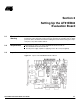
AT91EB42 Evaluation Board .............................................................................
Table of Contents Section 1 Overview............................................................................................... 1-1 1.1 1.2 1.3 Scope........................................................................................................1-1 Deliverables ..............................................................................................1-1 The AT91EB42 Evaluation Board .............................................................
Table of Contents Section 5 Appendix A – Configuration Straps....................................................... 5-1 5.1 5.2 5.3 5.4 Configuration Straps (CB1 - 23, JP1 - 8) ..................................................5-1 Power Consumption Measurement Strap (JP5) .......................................5-4 Ground Links (JP6) ...................................................................................5-4 Increasing Memory Size ................................................................
Section 1 Overview 1.1 Scope The AT91EB42 Evaluation Board enables real-time code development and evaluation. It supports the AT91M42800. This guide focuses on the AT91EB42 Evaluation Board as an evaluation and demonstration platform: Section 1 provides an overview. 1.2 Deliverables Section 2 describes how to set up the evaluation board. Section 3 details the on-board software. Section 4 contains a description of the circuit board.
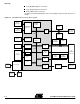
Overview 2 x 32-pin EBI expansion connectors 2 x 32-pin I/O expansion connectors 20-pin JTAG interface connector If required, user-defined peripherals can also be added to the board. See Section 5 for details. Figure 1-1. AT91EB42 Evaluation Board Block Diagram AT91M42800 Reset Controller JTAG ICE Connector 8K Byte RAM SRAM ARM7TDMI Processor EBI Expansion Connector EBI ASB 32.
Section 2 Setting Up the AT91EB42 Evaluation Board 2.1 Electrostatic Warning The AT91EB42 Evaluation Board is shipped in protective anti-static packaging. The board must not be subjected to high electrostatic potentials. A grounding strap or similar protective device should be worn when handling the board. Avoid touching the component pins or any other metallic element. 2.
Setting Up the AT91EB42 Evaluation Board 2.4 Jumper Settings JP1 is used to boot standard or user programs. For standard operations, set it in the STD position. JP8 is used to select the core power supply of the AT91M42800: 3.3V or 1.8V. For operation at 1.8V, MCK frequency shall be limited to 17 MHz. For more information about jumpers and other straps, see Section 5. 2.5 Powering Up the Board DC power is supplied to the board via the 2.1 mm socket (J1) shown in Figure 2-2.
Section 3 The On-board Software 3.1 AT91EB42 The AT91EB42 Evaluation Board embeds an AT49BV1604 Flash memory device proEvaluation Board grammed with default software. Only the lowest 8 x 8 KB sectors are used. The remaining sectors are user definable, and can be programmed using one of the Flash downloader solutions offered in the AT91 library.
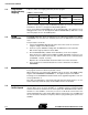
The On-board Software 3.3 Programmed Default Memory Mapping Table 3-1 defines the mapping defined by the boot program. Table 3-1. Memory Map Part Name Start Address End Address Size Device U1 0x01000000 0x011FFFFF 2M Bytes Flash AT49BV1604 U2-U3 0x02000000 0x02040000 256K Bytes SRAM The boot software program, FTS and SRAM downloader are in sectors 1 and 2 of the Flash device. Sectors 2 to 8 support the Angel Debug Monitor.
Section 4 Circuit Description 4.1 AT91M42800 Processor Figure 6-1 on page 6-2 shows the AT91M42800. The footprint is for a 144-pin TQFP package. Strap CB20 enables the user to choose between the standard ICE debug mode and the JTAG boundary scan mode of operation. The operating mode is defined by the state of the JTAGSEL input detected at reset.
Circuit Description 4.3 Memories The schematic (Figure 6-3 on page 6-4 in Section 6, “Appendix B – Schematics”) shows one AT49BV1604 2 MB 16-bit Flash, one AT45DB321 4 MB serial DataFlash, one AT24C512 64 KB EEPROM, one AT25256 32 KB EEPROM and two 128K/512K x 8 SRAM devices. Note: The AT91EB42 is fitted with two 128K x 8 SRAM devices.
Circuit Description of watchdog time-out as the pin NWDOVF of the AT91M42800 is connected to its input MR. The assertion of this reset signal will light up the red RESET LED (D10). By pressing the CLEAR RESET push button (S1), the LED can be turned off. Another supervisory circuit initializes separately the microcontroller-embedded JTAG/ICE interface when the 3.3V supply voltage drops below 3.0V. Note that this voltage can be changed, depending on the board production series.
Circuit Description 4-4 AT91EB42 Evaluation Board User Guide
Section 5 Appendix A – Configuration Straps 5.1 Configuration Straps (CB1 - 23, JP1 - 8) By adding the I/O and EBI expansion connectors, users can connect their own peripherals to the evaluation board. These peripherals may require more I/O lines than available while the board is in its default state. Extra I/O lines can be made available by disabling some of the on-board peripherals or features. This is done using the configuration straps detailed below.
Appendix A – Configuration Straps CB7 Closed Standard Power Supply Supervisory Enabling (1) Open Standard power supply is not connected to the ADC (U20) channel 2. This authorizes users to connect the corresponding ADC channel to their own resources via the I/O expansion connector. CB6, CB8 Closed (1) ADC Channels 3 and 4 Enabling ADC (U20) channels 3 and 4 are connected to ground. Open ADC (U20) channels 3 and 4 are not connected to ground.
Appendix A – Configuration Straps CB15 Serial DataFlash Enabling Closed(1) AT91 NPCSA0 select signal is connected to the serial DataFlash memory. Open AT91 NPCSA0 select signal is not connected to the serial DataFlash memory. This authorizes users to connect the corresponding PIO to their own resources via the I/O expansion connector. CB17 Closed SPI EEPROM Enabling (1) EEPROM communication enabled Open EEPROM communication disabled.
Appendix A – Configuration Straps JP1 User or Standard Boot Selection 2-3 The first half part of the Flash memory is accessible at its base address. 1-2 The second half part of the Flash memory is accessible at its base address. This authorizes users to download their own application software in this part and to boot on it. JP2 Push Button Enabling Open SW1-4 inputs to the AT91 are valid. Closed SW1-4 inputs to the AT91 are not valid.
Section 6 Appendix B – Schematics 6.1 Schematics The following schematics are appended: • Figure 6-1. PCB Layout • Figure 6-2. AT91EB42 Blocks Overview • Figure 6-3. EBI Memories • Figure 6-4. I/O and EBI Expansion Connectors • Figure 6-5. Push Buttons, LEDs and Serial Interface • Figure 6-6. AT91M42800 • Figure 6-7. Reset and JTAG Interface • Figure 6-8. Power Supply and Battery Charger • Figure 6-9. Battery Type and Connection • Figure 6-10.
Appendix B – Schematics Figure 6-1.
A20 PB22 IOB_32 IOB_52 EBI_[0..42] EBI_[0..42] IOB_[0..57] IOB_[0..57] EBI_41 IOB_[54..57] IOB_16 IOB_15 IOB_14 IOB_13 IOB_12 IOB_11 IOB_3 IOB_49 IOB_50 IOB_46 IOB_47 memories connected on EBI NRST VIN[1..4] NPCSA2 NPCSA1 NPCSA0 MOSIA MISOA SPCKA IRQ3 PB19 PB20 PB16 PB17 SERIAL MEMORIES MICROCONTROLLER IOB_[0..53] IOB_[0..53] IOB_[0..57] IOB_[0..57] INPUT / OUTPUT ON BOARD IOB_51 IOB_[36..45] EBI_[0..42] EBI_[0..42] IOB_[6..7] IOB_[9..10] IOB_0 micro / Rst / Wchdog / JTAG co. PB21 PB[6..
6-4 9 10 14 13 25 24 23 22 21 20 19 18 8 7 6 5 4 3 2 1 48 17 16 15 NRST_1 D5 D6 E6 E5 F6 C3 E4 F5 B3 H6 A5 A3 H2 G3 A2 H5 H4 NCS0_1 NRST_1 A17 A18 A19 D2 G4 C1 B2 F4 A4 A1 A0 A1 A2 A3 A4 A5 A6 A7 A8 A9 A10 A11 A12 A13 A14 A15 A16 12 N C S 0 _ 1 26 11 28 VCC3V3 R2 100k 2 2 NRD NWR0 CB10 2 1 A6 G6 1 NRST CB9 2 NCS1 VCC3V3 1 R1 100k VCC3V3 A1 A2 A3 A4 A5 A6 A7 A8 A9 A10 A11 A12 A13 A14 A15 A16 A17 A18 A19 1 NCS0 NWE NOE A20B A[0..
Appendix B – Schematics Figure 6-4.
SW3 1 R17 100K JP3 jumper_NO VAL_RS232 PA7 PA10 VCC3V3 D31 GREEN LED R75 100R VCC3V3 D32 GREEN LED R76 100R R74 100R D30 ORANGE LED VCC3V3 100nF 2 PB7 PB6 PB21 6 8 11 RXD0 RXD1 TXD0 TXD1 C22 100nF C18 100nF VCC3V3 PA0 3 74LV125D TCLK5 TCLK0 TIOA0 IRQ0 14 1 15 10 13 12 6 5 4 2 MAX3223ECAP U10 PB21 INVALID R1IN R2IN T1OUT T2OUT V- V+ FORCEOFF 100nF C16 R44 100k R43 100k FORCEON EN R1OUT R2OUT T1IN T2IN C2- C2+ C1- C1+ R45 100k R42 100k VCC3V3 GND
1 CB12 PA27 VCC3V3 AT91EB42 Evaluation Board User Guide 59 58 57 56 55 54 53 D15 D14 D13 52 51 50 GND VDDIO GND GND 49 48 D12 D11 D10 D9 D8 D7 D6 D5 D4 D[0..15] PB0 / NCS2 PB1 / NCS3 61 60 A[0..19] TCLK2 TIOB1 TIOA1 TCLK1 TIOB0 TIOA0 TCLK0 EBI_[0..15] GND VDDIO 70 69 68 67 66 65 64 63 62 EBI_[16..35] PB12 / PB11 / PB10 / PB9 / PB8 / PB7 / PB6 / TCLK5 TIOB4 TIOA4 TCLK4 TIOB3 TIOA3 TCLK3 TIOB2 TIOA2 VDDCORE 100nF VDDIO VDDCORE CTL[0..
6-8 NWDOVF C78 10pF C84 10pF JTAG4 1 MR VCC 100nF C94 3 4 CTL6 NRST C85 10pF C79 10pF JTAG1 S1 B.P. 74LVC74AD MR VCC 3 4 100nF 100nF JTAG4 9 JTAG3 19 17 15 13 11 7 5 JTAG1 JTAG2 3 NRST R27 100k 1 JTAGSEL VCC3V3 JTAGSEL MAX6315US30D4-T RST GND U13 C53 C52 9 8 5 6 JTAG0 2 1 10 11 12 13 C81 10pF JTAG3 R78 100K VCC3V3 C80 10pF JTAG2 MAX6315US30D4-T RST GND U14 PBRST 2 SW5 TP 33 JTAG0 U6B 4 CLEAR RST LED 74LVC02AD 1 S C1 1D R U12 7 JTAG[0..
AT91EB42 Evaluation Board User Guide C61 1 F 1 2 2 5 LT1503CS8-1.8 SHDN/SS C1- C1+ Vin U17 Vbatt- GND C2- C2+ Vout 7 8 6 1 10nF C62 1 F 6 7 5 1 16 + C103 10nF C63 10 F / 16V TLO Temp THI Vlimit REF FASTCHG V+ 11 3 1 10K CTN R58 10K R59 4k7 8 15 150R CC 4 TC C102 V+ R30 Batt- PGM1 PGM0 PGM3 PGM2 Batt+ 12 4 3 10 9 2 Vbatt+ 2R5 / 1W R62d R62c 10R 10R Vbatt- 2 V+ 2 1 CB22 1 CB23 2 Vbatt- Vbatt+ 1 CB21 5 cel.
Appendix B – Schematics Figure 6-9. Battery Type and Connection Battery : 6V / 300mAH NiCd Wire: gauge 20 AWG 1 J2 con. fem.
AT91EB42 Evaluation Board User Guide PB20 VIN[1..
Atmel Headquarters Atmel Operations Corporate Headquarters Atmel Colorado Springs Europe Atmel Rousset 2325 Orchard Parkway San Jose, CA 95131 TEL (408) 441-0311 FAX (408) 487-2600 Atmel U.K., Ltd. Coliseum Business Centre Riverside Way Camberley, Surrey GU15 3YL England TEL (44) 1276-686-677 FAX (44) 1276-686-697 1150 E. Cheyenne Mtn. Blvd.