AT91SAM9XE-EK Evaluation Board ....................................................................................................................
Table of Contents Section 1 Overview .................................................................................................................... 1-1 1.1 Scope................................................................................................................................. 1-1 1.2 Deliverables ....................................................................................................................... 1-1 1.3 AT91SAM9XE-EK Evaluation Board ..............................
Table of Contents (Continued) 4.3 Microcontroller Clock ......................................................................................................... 4-2 4.4 Memory Configuration........................................................................................................ 4-2 4.5 Ethernet ............................................................................................................................. 4-3 4.6 Miscellaneous ............................................
Section 1 Overview 1.1 Scope The AT91SAM9XE-EK evaluation kit enables the evaluation of and code development for applications running on an AT91SAM9XE device. This guide focuses on the AT91SAM9XE-EK board as an evaluation platform. The board supports the AT91SAM9XE in an LFBGA217 package as well as in a PQFP208 package. 1.2 Deliverables The AT91SAM9XE-EK package contains the following items: 1.
two user input push buttons one Wakeup input push button one reset push button one DataFlash, SD/MMC card slot four expansion connectors (PIOA, PIOB, PIOC, IMAGE SENSOR) one BGA-like EBI expansion footprint connector one Lithium Coin Cell Battery Retainer for 12 mm cell size 1-2 6311A–ATARM–04-Feb-08 AT91SAM9XE-EK Evaluation Board User Guide
Section 2 Setting Up the AT91SAM9XE-EK Board 2.1 Electrostatic Warning The AT91SAM9XE-EK evaluation board is shipped in protective anti-static packaging. The board must not be subjected to high electrostatic potentials. A grounding strap or similar protective device should be worn when handling the board. Avoid touching the component pins or any other metallic element. 2.2 Requirements In order to set up the AT91SAM9XE-EK evaluation board, the following items are needed: 2.
Figure 2-1.
Figure 2-2.
2.4 Powering Up the Board The AT91SAM9XE-EK requires 5V DC (±5%). DC power is supplied to the board via the 2.1 mm by 5.5 mm socket J1. Coaxial plug center positive standard. 2.5 Backup Power Supply The user has the possibility to plug a battery (3V Lithium Battery CR1225 or equivalent) in order to permanently power the backup part of the device. In this case, J10 configuration must be set in position 1, 2. Refer to Section 4.1. 2.
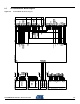
2.7 AT91SAM9XE-EK Block Diagram Figure 2-3.
Section 3 Board Description 3.
• Fully-featured System Controller, including • • • • • • • • • • • • • • • • • – Reset Controller, Shutdown Controller – Four 32-bit Battery Backup Registers for a Total of 16 Bytes – Clock Generator and Power Management Controller – Advanced Interrupt Controller and Debug Unit – Periodic Interval Timer, Watchdog Timer and Real-time Timer Reset Controller (RSTC) – Based on a Power-on Reset Cell, Reset Source Identification and Reset Output Control Clock Generator (CKGR) – Selectable 32,768 Hz Low
• Two Two-wire Interfaces (TWI) – Master, Multi-master and Slave Mode Operation – General Call Supported in Slave Mode – Connection to PDC Channel to Optimize Data Transfers in Master Mode Only • IEEE® 1149.1 JTAG Boundary Scan on All Digital Pins • Required Power Supplies: – 1.65V to 1.95V for VDDBU, VDDCORE and VDDPLL – 1.65V to 3.6V for VDDIOP1 (Peripheral I/Os) – 3.0V to 3.6V for VDDIOP0 and VDDANA (Analog-to-digital Converter) – Programmable 1.65V to 1.95V or 3.0V to 3.
NRST PIT MCI RSTC SHDC RTT PDC TWI0 TWI1 4GPREG PDC BOD POR VDDCORE OSC RC WDT OSC PLLB PLLA PMC PDC DBGU AIC System Controller POR Filter VDDBU SHDN WKUP OSCSEL XIN32 XOUT32 XIN XOUT PLLRCA DRXD DTXD PCK0-PCK1 FIQ IRQ0-IRQ2 TST SLAVE PIOC PIOB PIOA PDC USART0 USART1 USART2 USART3 USART4 NT R TD ST TDI TMO TC S RTK CK E SE L In-Circuit Emulator MMU TC0 TC1 TC2 ROM 32 Kbytes Bus Interface PDC SPI0 SPI1 Flash 128, 256 or 512 Kbytes I ICache 8 Kbytes TC3 TC4 T
3.3 Microcontroller One LFBGA 217-ball device fitted on board One LQFP 208-lead device footprint To use the microcontroller in the LQFP package, the user has to unsolder MN4 and solder the PQFP208 microcontroller on the MN6 footprint. 3.4 3.5 3.6 3.7 3.8 3.
socket 3.10 3.11 3.12 3.13 USB V2.0 full-speed compliant, 12 Mbits per second (UDP) Two(1) USB Host ports V2.
3.14 PIO Usage Table 3-1. PIO Controller A I/O Line Peripheral A Peripheral B Comments Function PA0 SPI0_MISO MCDB0 SPI DATAFLASH, SPI/MCI SD/MMC/DATAFLASH Slot PA1 SPI0_MOSI MCCDB (PA0..
Table 3-2. PIO Controller B I/O Line Peripheral A Peripheral B PB0 SPI1_MISO TIOA3 Audio DAC AT73C213 (MISO) PB1 SPI1_MOSI TIOB3 Audio DAC AT73C213 (MOSI) PB2 SPI1_SPCK TIOA4 Audio DAC AT73C213 (SPCK) PB3 SPI1_NPCS0 TIOA5 Audio DAC AT73C213 (Chip Select) PB4 TXD0 COM PORT 0 (TXD) PB5 RXD0 COM PORT 0 (RXD) PB6 TXD1 TCLK1 COM PORT 1 (TXD) PB7 RXD1 TCLK2 COM PORT 1 (RXD) PB8 TXD2 PB9 RXD2 PB10 TXD3 ISI_D8 (J28) IMAGE SENSOR CONNECTOR (PB10..
Table 3-3.
Section 4 Configuration 4.1 Jumpers Table 4-1. Jumpers Configuration Designation Default Setting Feature J2 Closed 3.3V Jumper(1) J3 Closed Forces power on. To use the software shutdown control, J3 must be opened. 3V battery backup must be present.
4.2 JTAG/ICE Table 4-2. JTAG/ICE Configuration 4.3 Designation Default Setting Feature S1 Opened Disables the ICE NTRST input S2 Opened Selects ICE mode or JTAG mode S3 Opened Disables TCK <-> RTCK local loop. If S3 is closed, R13 must be unsoldered. R13 Soldered Enables the ICE RTCK return. S3 must be opened R14 Soldered Enables the ICE NRST input Microcontroller Clock Table 4-3.
4.5 Ethernet RMII is the factory default mode. To evaluate the MII mode, the user has to unsolder R49, R50, R127, close S7, S8 and populate R119 to R126, C88, C89, Y4. 4.6 Miscellaneous Refer to the TOP level schematic for the PIO usage. Table 4-5. Miscellaneous Designation Default Setting R82 Soldered R72 Soldered R73 Soldered Feature USB DEVICE: Enables the use of the USBCNX signal DBGU COM Port: Enables the use of DTXD output signal. Enables the use of DRXD input.
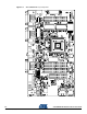
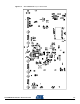
Section 5 Schematics 5.
Section 6 Revision History 6.1 Revision History Table 6-1. Document Comments 6311A First issue. AT91SAM9XE-EK Evaluation Board User Guide Change Request Ref.
6-2 6311A–ATARM–04-Feb-08 AT91SAM9XE-EK Evaluation Board User Guide
Headquarters International Atmel Corporation 2325 Orchard Parkway San Jose, CA 95131 USA Tel: 1(408) 441-0311 Fax: 1(408) 487-2600 Atmel Asia Room 1219 Chinachem Golden Plaza 77 Mody Road Tsimshatsui East Kowloon Hong Kong Tel: (852) 2721-9778 Fax: (852) 2722-1369 Atmel Europe Le Krebs 8, Rue Jean-Pierre Timbaud BP 309 78054 Saint-Quentin-enYvelines Cedex France Tel: (33) 1-30-60-70-00 Fax: (33) 1-30-60-71-11 Atmel Japan 9F, Tonetsu Shinkawa Bldg.