M1 System Management Board User’s Guide
Actel Corporation, Mountain View, CA 94043 © 2008 Actel Corporation. All rights reserved. Printed in the United States of America Part Number: 50200081-1 Release: November 2008 No part of this document may be copied or reproduced in any form or by any means without prior written consent of Actel. Actel makes no warranties with respect to this documentation and disclaims any implied warranties of merchantability or fitness for a particular purpose.
Table of Contents 1 Introduction . . . . . . . . . . . . . . . . . . . . . . . . . . . . . . . . . . . . 5 Design Example . . . . . . . . . . . . . . . . . . . . . . . . . . . . . . . . . . . . . . . . . . . 8 Document Contents . . . . . . . . . . . . . . . . . . . . . . . . . . . . . . . . . . . . . . . . . 8 2 Contents and System Requirements . . . . . . . . . . . . . . . . . . . . . . . 9 Kit Contents . . . . . . . . . . . . . . . . . . . . . . . . . . . . . . . . . . . . . . . . . . . . .
Table of Contents 6 Demonstration Scripts . . . . . . . . . . . . . . . . . . . . . . . . . . . . . . 41 General Setup . . . . . . Basic Controls . . . . . Voltage Monitoring . . . Current Monitoring . . . Temperature Monitoring RTC Control . . . . . . Logging Events . . . . . . . . . . . . . . . . . . . . . . . . . . . . . . . . . . . . . . . . . . . . . . . . . . . . . . . . . . . . . . . . . . . . . . . . . . . . . . . . . . . . . . . . . . . . . . . . . . . . . . . . . . . . . . . . .
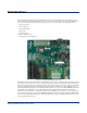
Introduction The Actel M1 System Management Board Development Kit provides an excellent platform for developing system management applications and/or applications with a microprocessor. The kit includes a CortexTM-M1-enabled Fusion device, a system management GUI, and a platform (Figure 1) for systems that performs the following functions: • Power-up detection • Power sequencing • Thermal management • Sleep modes • System diagnostics • Remote communications • Clock generation and management Figure 1.
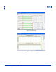
The system management GUI (Figure 2, Figure 3 and Figure 4) includes the following tabs: • Board status • Application data • IPMI data • Graphical display of analog data The GUI helps users to: • Monitor power supplies • Monitor temperature sensors • Set LEDs and text for display • Set and read the RTC • Display embedded Flash contents Figure 2.
Figure 3. Threshold Tab Figure 4.
Design Example This user’s guide utilizes the M1 System Management Board, the System Management software and examples to demonstrate System Management’s capabilities. It can also be used as a reference design to jumpstart user application designs, including a firmware platform for re-use. Design examples for the older CoreMP7-enabled board, featuring the M7AFS600 device, may still be found on the Actel web site. Only Cortex-M1-enabled designs should be used with the M1-SYSMGMT-DEV-KIT board.
1 Contents and System Requirements This chapter details the contents of the Cortex-M1-enabled Fusion-based System Management Kit and lists the necessary components required to use it. Kit Contents • M1 System Management Board • Switching brick power supply (rated from 110 V to 240 V AC) from 50 Hz to 60 Hz input, an providing 9 V DC output at up to 2 A, part number DTS090220UP5P-SZ from CUI, Inc. • Power cables and adapter • RS-232 cable • User’s guide Optional: • 7.
2 Hardware Components This chapter describes the hardware components of the M1 System Management Board. Power Supplies A 9 V power supply is provided with the kit. The 9 V brick is connected to the J1 connector on the board. This power supply feeds the input voltage of three LDO-type regulators—U1, U2, and U3—through a slide switch, SW7. The switch toggles between two positions On-Off. The regulators provide three voltages 5 V, 3.3 V and 1.5 V.
Hardware Components Clocks and Reset CLK Source A 50 MHz clock with 50 ppm stability is provided at location U5. This clock is the clock source for the A3P250-FG144 device at U24 (pin F12) and the M1AFS1500-FG484 device at location U23 (pin A3). A user clock is also provided at location U7. Any 3.3 V clock can be installed in the socket of this location. The user clock feeds only to the M1AFS1500-FG484 device. A 32.768 kHz crystal is provided at location Y1 on the board.
Programming Table 2-2 · Jumpers Settings for In-System Programming (Continued) Jumper Setting for In-System Programming JP14 1-2 JP15 1-2 JP16 1-2 JP17 1-2 JP10 (If PCI1 is not in chain) 1-2 JP11 (If PCI2 is not in chain) 1-2 M1AFS1500-FG484 to A3P Programming The board can be configured to program an A3P250 device with the M1AFS1500-FG484 device, see Figure 2-2. Table 2-3 shows the jumpers settings required. M1AFS1500-FG484 A3P250-FG144 Figure 2-2.
Hardware Components External Programming The System Management Board can program an external JTAG compliant device with the M1AFS1500-FG484 device. Figure 2-3 shows the external programming setup. See Table 2-4 for the jumper settings. Buffers Connector Cable M1AFS1500-FG484 External Device Figure 2-3.
LCD Display Push Buttons Five push buttons are provided at SW1, SW2, SW3, SW4 and SW5, see Figure 2-5. These push buttons are located near the LCD display and are used to navigate the LCD screen for different tests/demo scripts. These signals are driven to the A3P250 device. SW2 UP SW3 Select SW1 SW4 Right Left Down SW5 Figure 2-5. Push Buttons LCD Display An 8-bit, 16 x 2 character LCD display (part# LCMS01602DSFC) is provided on the board at LCD1.
Hardware Components Santa Cruz Connector Header A set of three headers ( J8, J9, and J11), per the Santa Cruz header specification, are provided for debug purposes and installing compatible daughter boards. All I/Os on the Santa Cruz header are shared with the PCI signals. Note: Do not exercise the PCI connector and the Santa Cruz connector header simultaneously.
Ports Ports RS232 This kit contains one RS-232 port with a MAX3221 transceiver that can be used for communications between the M1AFS1500-FG484 device and a common serial port found on a PC or other RS-232 compatible device. Note: The RS-232 interface does not support hardware RTS/CTS hand shaking. The default configuration has the RTS and CTS shorted together to create a loopback connection.
Hardware Components ATX Connector Supply The ATX connections demonstrate the analog function features of the M1AFS1500-FG484 device. The functional description and pin out information is shown in Figure 2-8. All supplies on the ATX power supply can support a maximum of 10 A. Current Monitored Output Power Supply 12V 0.1 ohm 5V 3.3V 0.1 ohm 0.1 ohm External Board Power Supply 12V 3.3V Q14 Q15 AV0 AV1 AV2 AC0 AC1 AC2 Q13 5V AV8 AV7 AV9 M7AFS AG2 AG1 AG0 12V 5V 3.
ATX Connector Supply Table 2-8 · ATX Main Power Connector Pinout (Continued) Pin Number Signal Function 9 +5 VSB 10 +12 VDC 11 +3.3 VDC 12 –12 VDC 13 COM 14 PS_ON# 15 COM 16 COM 17 COM 18 N/C 19 5 VDC 20 5 VDC Note: Do not plug in the ATX supply to J73. Table 2-9 · ATX Main Power Connect Pinout by Function Signal Function Pin Number +3.3 VDC 1 +3.3 VDC 2 +3.
Hardware Components Table 2-9 · ATX Main Power Connect Pinout by Function (Continued) Signal Function Pin Number COM 16 COM 17 N/C 18 PS_ON# 14 PWR_OK 8 PS_ON# Signal The ATX supply plugs in to the J72 connector. The PS_ON# signal is the main switch for the ATX supply. The signal logic is controlled by the signal AFS_PS_ON on the M1AFS1500-FG484 device.
ATX Connector Supply Table 2-12 · Gate Driver Settings AG FET Output Voltage Tristate Off 0V On On 12 V, 5 V, 3.3 V Note: The gate driver has to be configured as a constant current sink with a 10-μa or 30-μa drive level to get different ramp-rates. Power-Out Connectors The output voltage of the FETs goes to two different power-out connectors: ATX Connector J73 – Any external daughter board can be plugged into this connector.
Hardware Components Dummy Loads Dummy loads can be connected to the output voltages to demonstrate the capability of the M1AFS1500-FG484 device to monitor current in the absence of an external daughter board. Connect the dummy loads as shown in Table 2-15. Table 2-15 · Dummy Loads Settings Reference Designator Load Output Voltage Approximate Current JP32 110 Ω 12 V 109 mA JP33 39 Ω 5V 128 mA JP34 39 Ω 3.
Temperature Diodes from 0 V to 5 V using the knob control (Figure 2-9). Voltage Increase Voltage Decrease Figure 2-9. Potentiometer Knob Control Tri-Color LED A tri-color LED (AAF5060PBESEEVG) is provided on the board. The LED has three colors—blue, orange, and green—controlled by three gate driver (AG) pins from the M1AFS1500-FG484 device. A combination of colors can be turned On to form new colors.
Hardware Components Heater/FAN Loads The board has two loads controlled by the gate drivers from the M1AFS1500-FG484 device: heater and fan. VCC Q11 AG Load Figure 2-10. Heater/ Fan Loads. Table 2-18 · AG Pads Settings AG Pads (M1AFS1500-FG484) LED Tristate Off On-High Current Drive On Note: Set the AG pad in a high current drive mode, which can sink 25 mA. Heater A 7.5 Ω wire-wound resistor (R106) is provided on the board.
Digital Brick for EXT_VOL[3]. Identical switch positions are used for common division factors across all three switches. The table below applies to any switch. Table 2-19 · Switch Settings Numerical Switch Position Internal Voltage as Factor of External Voltage Vext 1 Vext * 1 2 Vext * 1/2 3 Vext * 1/4 4 Vext * 1/8 Note: If an external board has voltages greater than 12 V that need to be monitored, use these options to apply the right range of voltage to the AV pad.
Hardware Components TRIM_VOL This pin is an input to the digital brick controlled by the M1AFS1500-FG484 I/O with a PWM control. The PWM output can be configured using different RC values on the surface mount pads (Figure 2-12). 5 V Power R224 R207 AFS Pad R206 TRIM_VOL C36 Figure 2-12. TRIM_VOL This pin can be used to trim the output voltage of the digital brick. The trim voltage varies based on the type of digital brick being used.
Test Points Charging and Discharging Routines The battery is charged/discharged using the two FET controls (Figure 2-13). When Q3 is turned On and Q2 is turned Off, the constant current source (20 mA) will slowly charge up the 7.2 V battery. When Q3 is turned Off and Q2 is turned On, the battery is placed in discharge mode and will power up the board and start discharging. All voltages and current are monitored by the M1AFS1500-FG484 device.
Hardware Components Table 2-21 · Test Points by Numerical Sequence (Continued) Test Points Signal Name TP4 Digital 3.3 V TP5 1.5 V EXT TP6 1.5 V TP9 Main 3.3 V TP10 1.5 V TP11 Analog GND TP12 VIN_D TP13 Main GND TP14 5V TP15 VIN TP16 Analog 3.3 V TP17 Analog GND TP18 ATX output 12 V TP19 ATX output 5 V TP24 ATX Output 3.3 V Table 2-22 · Test Points in Signal Name Order Signal Name 28 Test Points 1.5 V TP6 1.5 V TP10 1.5 V EXT TP5 5V TP14 Analog 3.
Prototype Section Table 2-22 · Test Points in Signal Name Order (Continued) Signal Name Test Points Digital GND TP3 Main 3.3 V TP9 Main GND TP13 VIN TP15 VIN_D TP12 Prototype Section A prototype section is provided at the bottom of the board for debug and development purposes (Figure 2-14). The section is 20 holes x 20 holes large with the hole size at 0.100 in x 0.100 in, center to center.
Hardware Components The following signals are provided in the debug area: • Power: 5 V, 3.3 V, 1.5 V and digital and analog GND are provided in this are for easy access. Ensure that the current consumption for any part added to this does not exceed 500 mA. • Spare I/Os: 24 I/Os are provided for debug purposes. These I/Os are connected to the A3P250-FG144 FPGA part. • Gate Driver: Three gate driver pins are provided: IO_BLUE_TRI, IO_GREEN_TRI, IO_ORANGE_TRI.
3 System Management Software The System Management software has scrollable, zoomable, and sizeable real-time updated diagrams that enable the simultaneous monitoring of the voltages, currents, and temperatures throughout the board. You can also set the thresholds for these variables and log specific events, when they breach a target level.
System Management Software Board Status The Board Status tab is split into ten panels that control the behavior of the board (Figure 3-2). Figure 3-2. Board Status Tab LEDs To turn on and off each LED on the board, click the corresponding LED button in the software. LCD To output two lines of text to the LCD screen, type the text that you want to display and click the Set to button. The board firmware also uses the LCD and displays the “Clock”.
Board Status Controls To display the state (open or closed) of the on-board DIP switches, open and close the DIP switches on the board. The results are displayed in the software. To display the potential difference across the potentiometer, adjust the rotating switches on the board. The results are displayed in the software. Board Supply The board supply displays a real-time reading of the voltage and current ratings for the main supply. It also displays the real-time voltages for the 1.5 V, 3.3 V, and 5.
System Management Software Graphs The Graphs tab generates the graphs for the various voltages, currents, and temperatures involved on the board (Figure 3-3). Figure 3-3. Graphs Tab The Zoom box allows you to zoom in, zoom out, zoom fit, or zoom reset the graphs. To turn the graph background from the default black to white, check the appropriate box in the Background box. The scale in percentages to the left of each graph corresponds to the absolute measured range for any of the displayed graphs.
Comms (see “Thresholds” on page 36). The timestamp is based on the time set on the board at the instant the event occurred. The events show all crossing of thresholds (including returning to normal). See “Event Log Tab” on page 35. Figure 3-4. Event Log Tab To upload the stored event log from the target board, click the Update button. Refer to “To set up sample/threshold data logging:” on page 46 for more information about setting up event logging.
System Management Software The raw data window displays raw data based on the transmitted bit sequences (Figure 3-5). Figure 3-5. Comms Tab Thresholds The Thresholds tab allows you to adjust thresholds for which events are logged (Figure 3-6). Figure 3-6.
Thresholds • Lo-Warn is a local minimum, which produces a YELLOW light if breached. • Hi-Warn is a local maximum, which if passed also produces a YELLOW light. • Hi-Limit is the absolute maximum, which produces a RED light if breached. When the thresholds are set between Lo-Warn and Hi-Warn, a green light indicates that the board is operating at optimum levels between these two points. The shaded boxes on the right display the exact threshold values for the Lo-Limit, Lo-Warn, Hi-Warn and Hi-Limit.
4 Setting Thresholds This section details how to set the thresholds used throughout the demonstration. The board thresholds can be set in two different ways in the Thresholds tab: you can set and see the points and triggers graphically or you can use the highwater/low-water slider marker, which will allow tracking of extreme values. Setting the Thresholds Graphically 1. Click the Graphs tab. 2.
Setting Thresholds Setting the Thresholds with the Slider Marker 1. Click the Thresholds tab. 2. Select the part for which you wish to alter the threshold levels. 3. Set the Lo-Warn and Hi-Warn levels as desired. 4. Set the Lo-Limit and Hi-Limit levels as desired. Figure 4-2. Setting Thresholds by Slide Marker Voltage, Current, and Temperature Status Indicators The following explains the voltage, current, and temperature status indicators found in the Board Status tab next to each reading.
5 Demonstration Scripts The scripts in this chapter demonstrate some of the basic functions of the board and the System Management software, including the following: • General setup • Basic controls • Voltage monitoring • Current monitoring • Temperature monitoring • RTC control • Logging events General Setup This section describes how to set up the System Management board and software using an external power supply brick. 1.
Demonstration Scripts Figure 5-3. ATX Power Supply 2. Using the RS-232 cable supplied, connect one end to the on-board RS-232 port and the other end to serial COM Port 1 (recommended) on the host PC. 3. Power-on the board controller. Note: The power connector can only be inserted in one way, with the tag facing towards the LCD screen. 4. Press the global reset (GL_RESET) button on-board before every demonstration (Figure 5-4). 5. Start the System Management software. 6.
Basic Controls Basic Controls This section demonstrates simple on-board functions. 1. Set up the board, as indicated in “General Setup” on page 41. 2. Start the System Management software, and click the Board Status tab. 3. Click each LED, one through 12. This individually lights up the LEDs on the board. LEDs 0 to 7 are shown in Figure 5-5. LEDs 8 to 12 are scattered around the board. Figure 5-5. LEDs 0-7 4. Press the push buttons on the top left of the board.
Demonstration Scripts Voltage Monitoring This section demonstrates how to use the System Management software to monitor the board's voltages with the external power supply. 1. Observe voltages in real-time (including potentiometer) in the Board Status tab (Figure 5-9). 2. View the graphs in the Graphs tab. If necessary, scroll down to view the desired graph. Note that the graph may change slowly upon connection to power. 3. Observe the reading for Main Supply in the Board Supply panel (Figure 5-9).
Temperature Monitoring 3. Remove the load resistors (pull on the black plastic tab, shown in Figure 5-11). Observe the currents (3.3 V, 5.0 V, and +12 V) in the PSU Supply panel on the Board Status tab. Figure 5-11. Load Resistors 4. Observe the graph as the load is removed. Note the current goes to 0 mA. 5. Compare the readings in the Board Supply and PSU Supply panels to their corresponding graphs in the Graphs tab.
Demonstration Scripts To upload a stored event log from the target board, click the Update button. This takes all the current board information from the internal Fusion Flash nonvolatile memory and displays it on-screen with specific details about type, channel, timestamp, and description. Description may include source, time, and historic data. To set up sample/threshold data logging: 1. Click the Thresholds tab and set the threshold for the potentiometer. Ensure the potentiometer is in range.
A M1AFS1500-FG484 Pin List This pin list is also applicable to the older SYSMGMT-DEV-KIT fitted with an M7AFS600-FG484 device. Pin usage is the same on these kits. A1 Ball Pad Corner 22 21 20 19 18 17 16 15 14 13 12 11 10 9 8 7 6 5 4 3 2 1 A B C D E F G H J K L M N P R T U V W Y AA AB Figure A-1. 484-Pin FBGA (Bottom View) Note: Full pin list data for the 484-Pin FBGA package is available in the Fusion datasheet, at http://www.actel.com/documents/Fusion_DS.
M1AFS1500-FG484 Pin List Table A-1 · Subset of M1AFS1500-FG484 Pin List Usage Specific to System Management Board 48 A9 SSRAM_CSN A10 FLASH_READN/SSRAM_READN Shared A11 MEM_ADDR[8] A12 IO_AFS_TX A13 SDA1 A14 FPGA-ENA-TXD[2] A15 MEM_DATA[12] A16 FPGA_ENA_MDC A17 FPGA_ENA_RXCLK A18 RS485_RO A19 RVI-ME-RCK A20 RVI-ME-DBGRQ B3 FPGA_ENA_RXER B5 MEM_ADDR[10] B6 MEM_ADDR[19] B8 MEM_ADDR[9] B9 SSRAM_B2N B11 MEM_DATA[3] B12 FPGA_ENA_RXD[1] B14 AFS_PS_ON B17 GL_RESET C1 S
Table A-1 · Subset of M1AFS1500-FG484 Pin List Usage Specific to System Management Board C22 FPGA_ENA_RXD[3] D1 SSRAM_B1N D3 MEM_DATA[5] D4 SSRAM_CLK D5 RVI-ME-nSRST D6 RVI-ME-nTRST D7 SSRAM_B3N D8 MEM_DATA[6] D9 MEM_DATA[4] D10 MEM_ADDR[1] D11 RS484_DI D12 FPGA_ENA_CRS D14 FPGA_ENA_MDIO D15 FLASH_CSN D16 FPGA_ENA_TXCLK D17 FPGA_ENA_TXEN D20 FPGA_ENA_RXD[0] D22 AFS_MB_PS_ON E1 MEM_DATA[8] E2 MEM_DATA[9] E4 RVI-ME-TCK E5 RVI-ME-TDI E11 MEM_ADDR[15] E12 AFS_TDO
M1AFS1500-FG484 Pin List Table A-1 · Subset of M1AFS1500-FG484 Pin List Usage Specific to System Management Board 50 F14 MEM_ADDR[16] F19 RS485_REB/AFS_TRST F20 AD[3] F21 AD[11] F22 AD[10] G1 MEM_DATA[21] G3 MEM_DATA[11] G4 MEM_DATA[22] G9 MEM_ADDR[18] G10 MEM_ADDR[11] G11 PCIREQN[1] G19 AD[2] G20 AD[6] G22 AD[7] H1 MEM_DATA[19] H2 IO_FET_FAN H4 MEM_DATA[23] H5 MEM_ADDR[12] H18 MEM_DATA[2] H19 AD[4] H21 AD[26] H22 AD[9] J2 MEM_DATA[25] J3 MEM_DATA[26] J4 S
Table A-1 · Subset of M1AFS1500-FG484 Pin List Usage Specific to System Management Board K16 PCIPME[2] K20 AD[22] K22 AD[21] L1 MEM_DATA[14] L5 INTBN L7 PCISMBCLK L16 MEM_ADDR[13] L18 MEM_ADDR[17] L19 AD[17] L21 AD[20] L22 AD[5] M5 MEM_ADDR[0] M7 MEM_DATA[20] M16 MEM_ADDR[14] M18 MEM_ADDR[2] M19 IN_POWER_OK M21 AD[0] M22 AD[19] N3 PCICLK N16 CBEN[0] N19 AD[28] N20 AD[12] N22 AD[8] P1 PCIGNTN[2] P2 INTAN P3 FRAMEN P4 MEM_DATA[28] P5 MEM_DATA[24] P16 ME
M1AFS1500-FG484 Pin List Table A-1 · Subset of M1AFS1500-FG484 Pin List Usage Specific to System Management Board 52 P22 AD[25] R1 MEM_DATA[17] R2 MEM_DATA[18] R4 MEM_DATA[27] R5 IRDYN R18 TRDYN R19 MEM_ADDR[7] R21 AD[24] R22 AD[18] T3 SERRN T4 M66EN T10 BAT_DISCHARGE_MON_AV T12 AV_PSU_N12V T13 AV_POT T19 RVI-ME-TDO T20 RS232_TX0 T22 AD[13] U1 PERRN U2 DEVSELN U3 PCIPME[1] U4 STOPN U10 BAT_DISCHARGEMON_AC U13 BAT_MODE U19 SSRAM_PWRDWN U20 RS485_DE/AFS_TDI
Table A-1 · Subset of M1AFS1500-FG484 Pin List Usage Specific to System Management Board V13 EXT_VOL2 W4 CBEN[2] W5 AD[31] W6 AV_PWR2_3.3V W8 AV_PWR2_5V W9 AV_PWR2_12V W11 BAT_CHARGE_MON_AV W12 AV_PSU_12V W14 AV_PSU_5V W15 AV_PSU_3.3V W17 VIN_BAT_AV Y1 CBEN[3] Y2 PCIRSTN Y3 CBEN[1] Y4 PAR Y6 AC_PWR2_3.3V Y8 AC_PWR2_5V Y9 AC_PWR2_12V Y11 BAT_CHARGEMON_AC Y12 SKP_5V Y14 SKP_3.3V Y15 1.5V Y17 VIN_BAT_AC AA6 AG_PSU_3.
M1AFS1500-FG484 Pin List Table A-1 · Subset of M1AFS1500-FG484 Pin List Usage Specific to System Management Board AB7 ATRN_REG AB8 EXT_VOL1 AB9 BAT_AT AB10 BAT_ATRN/ATRN_PCI AB11 AT3_PCI AB12 AT6_LCD AB14 EXT_VOL3 AB15 AT8_Heater AB16 ATRN_HEATER AB17 DIG_BRK_OUT1 Shared Table A-2 · Subset of M1AFS1500-FG484 Pin List Usage Specific to System Management Board by Function Order ARM Debugger RVI-ME-DBGACK C4 RVI-ME-DBGRQ A20 RVI-ME-nSRST D5 RVI-ME-nTRST D6 RVI-ME-RCK A19 RVI-ME
Table A-2 · Subset of M1AFS1500-FG484 Pin List Usage Specific to System Management Board by Function Order (Continued) Ethernet Pin Name FPGA_ENA_MDC A16 FPGA_ENA_MDIO D14 FPGA_ENA_COL P18 FPGA_ENA_RXCLK A17 FPGA_ENA_RXDV B18 FPGA_ENA_CRS D12 FPGA_ENA_RXER B3 FPGA_ENA_RXD[0] D20 FPGA_ENA_RXD[1] B12 FPGA_ENA_RXD[2] A4 FPGA_ENA_RXD[3] C22 FPGA_ENA_TXCLK D16 FPGA_ENA_TXEN D17 FPGA_ENA_TXD[0] C13 FPGA_ENA_TXD[1] C14 FPGA_ENA_TXD[2] A14 FPGA_ENA_TXD[3] B15 Gate Drivers Pin N
M1AFS1500-FG484 Pin List Table A-2 · Subset of M1AFS1500-FG484 Pin List Usage Specific to System Management Board by Function Order (Continued) GL_RESET B17 PCI 56 Pin Name AD[0] M21 AD[1] E22 AD[2] G19 AD[3] F20 AD[4] H19 AD[5] L22 AD[6] G20 AD[7] G22 AD[8] N22 AD[9] H22 AD[10] F22 AD[11] F21 AD[12] N20 AD[13] T22 AD[14] E21 AD[15] J19 AD[16] J22 AD[17] L19 AD[18] R22 AD[19] M22 AD[20] L21 AD[21] K22 AD[22] K20 AD[23] J20 AD[24] R21 AD[25] P22 AD[26
Table A-2 · Subset of M1AFS1500-FG484 Pin List Usage Specific to System Management Board by Function Order (Continued) AD[30] P21 AD[31] W5 CBEN[0] N16 CBEN[1] Y3 CBEN[2] W4 CBEN[3] Y1 DEVSELN U2 FRAMEN P3 INTAN P2 INTBN L5 INTCN V4 INTDN V1 IRDYN R5 M66EN T4 PAR Y4 PCICLK N3 PCIGNTN[1] V5 PCIGNTN[2] P1 PCIREQN[1] G11 PCIREQN[2] A8 PCIRSTN Y2 PERRN U1 SERRN T3 STOPN U4 TRDYN R18 CLK_VAR V2 PCIPME[1] U3 PCIPME[2] K16 PCISMBCLK L7 PCISMBDAT K4 RS232
M1AFS1500-FG484 Pin List Table A-2 · Subset of M1AFS1500-FG484 Pin List Usage Specific to System Management Board by Function Order (Continued) RS232_TX0 T20 RS485 RS484_DI D11 RS485_DE/AFS_TDI U20 RS485_REB/AFS_TRST F19 RS485_RO A18 SMBus Pin Name AFS_TDO E12 SCL1 C16 SCL2/AFS_TCK J4 SDA1 A13 SDA2/AFS_TMS E19 SRAM/FLASH 58 Pin Name Pin Name FLASH_CSN D15 FLASH_RB C9 FLASH_READN/SSRAM_READN Shared A10 FLASH_RPN C10 FLASH_WRITEN/SSRAM_BWRITTEN Shared A5 MEM_ADDR[0] M5 M
Table A-2 · Subset of M1AFS1500-FG484 Pin List Usage Specific to System Management Board by Function Order (Continued) MEM_ADDR[14] M16 MEM_ADDR[15] E11 MEM_ADDR[16] F14 MEM_ADDR[17] L18 MEM_ADDR[18] G9 MEM_ADDR[19] B6 MEM_DATA[0] J16 MEM_DATA[1] P16 MEM_DATA[2] H18 MEM_DATA[3] B11 MEM_DATA[4] D9 MEM_DATA[5] D3 MEM_DATA[6] D8 MEM_DATA[7] F2 MEM_DATA[8] E1 MEM_DATA[9] E2 MEM_DATA[10] F1 MEM_DATA[11] G3 MEM_DATA[12] A15 MEM_DATA[13] K3 MEM_DATA[14] L1 MEM_DATA[15] A7
M1AFS1500-FG484 Pin List Table A-2 · Subset of M1AFS1500-FG484 Pin List Usage Specific to System Management Board by Function Order (Continued) MEM_DATA[26] J3 MEM_DATA[27] R4 MEM_DATA[28] P4 MEM_DATA[29] K1 MEM_DATA[30] C7 MEM_DATA[31] C6 SSRAM_B0N C1 SSRAM_B1N D1 SSRAM_B2N B9 SSRAM_B3N D7 SSRAM_CLK D4 SSRAM_CSN A9 SSRAM_PWRDWN U19 Temperature Monitors AT0_REG AB6 AT3_PCI AB11 AT4_COPPER V11 AT6_LCD AB12 AT8_Heater AB15 ATRN_COPPER V12 ATRN_HEATER AB16 ATRN_REG AB7
Table A-2 · Subset of M1AFS1500-FG484 Pin List Usage Specific to System Management Board by Function Order (Continued) AV_PSU_5V W14 AV_PSU_N12V T12 AV_PWR2_12V W9 AV_PWR2_3.3V W6 AV_PWR2_5V W8 BAT_CHARGE_MON_AV W11 BAT_CHARGEMON_AC Y11 BAT_DISCHARGE_MON_AV T10 BAT_DISCHARGEMON_AC U10 DIG_BRK_OUT1 AB17 EXT_VOL1 AB8 EXT_VOL2 V13 EXT_VOL3 AB14 SKP_3.
B A3P250-FG144 Pin List A1 Ball Pad Corner 12 11 10 9 8 7 6 5 4 3 2 1 A B C D E F G H J K L M Figure B-1. 144-Pin FBGA (Bottom View) Note: Full pin list data for the 144-Pin FBGA package is available in the ProASIC3 datasheet, at http://www.actel.com/documents/PA3_DS.
A3P250-FG144 Pin List Table B-1 · Subset of A3P250-FG144 Pin List Usage Specific to System Management Board 64 B5 rx B6 tx B7 lcd_blk B9 led[7]-green B10 dip[0] B10 led[6]-green C1 led[5]-green C2 led[4]-green C3 led[3]-red C5 led[2]-red C6 led[1]-red C7 led[0]-red C8 key[0]-select C9 key[3]-right C10 key[4]-left C11 key[1]-down C12 key[2]-up D1 debug[10] D2 debug[9] D3 debug[8] D4 debug[7] D5 debug[6] D6 debug[5] D7 debug[4] D8 debug[3] D9 debug[2] D10
Table B-1 · Subset of A3P250-FG144 Pin List Usage Specific to System Management Board F4 led_pci F12 clk_50Mhz G1 PCI_PRSNT1 G4 PCI_PRSNT2 G8 sram_ft G9 lcd_tr G10 lcd_re G11 eth_rst H2 eth_an_en H3 eth_an1 H4 eth_an0 H6 lcd_db[7] H7 lcd_db[6] H8 lcd_db[5] H9 lcd_db[4] H11 lcd_db[3] J1 lcd_db[2] J2 lcd_db[1] J4 lcd_db[0] J5 lcd_rw J6 lcd_rs K1 debug[18] K2 debug[19] K3 debug[20] K4 debug[21] K5 debug[22] K6 debug[23] L3 clk_25Mhz M2 debug[17] M3 deb
A3P250-FG144 Pin List Table B-1 · Subset of A3P250-FG144 Pin List Usage Specific to System Management Board M7 debug[12] M8 debug[11] Table B-2 · Subset of A3P250-FG144 Pin List Usage Specific to System Management Board by Function Order Clocks and Resets clk_25Mhz L3 clk_50Mhz F12 gl_reset E2 CoreUART(A3P-M1AFS) Pin Name rx B5 tx B6 DIP Switch Pin Name dip[0] B10 dip[1] A11 dip[2] A10 dip[3] A9 dip[4] A7 dip[5] A5 dip[6] A4 dip[7] A3 Ethernet Pin Name eth_an_en H2 et
Table B-2 · Subset of A3P250-FG144 Pin List Usage Specific to System Management Board by Function Order LCD Display Pin Name lcd_blk B7 lcd_db[0] J4 lcd_db[1] J2 lcd_db[2] J1 lcd_db[3] H11 lcd_db[4] H9 lcd_db[5] H8 lcd_db[6] H7 lcd_db[7] H6 lcd_re G10 lcd_rs J6 lcd_rw J5 lcd_tr G9 LEDs Pin Name led[0]-red C7 led[1]-red C6 led[2]-red C5 led[3]-red C3 led[4]-green C2 led[5]-green C1 led[6]-green B10 led[7]-green B9 led_copper F1 led_heater E11 led_lcd F3 le
A3P250-FG144 Pin List Table B-2 · Subset of A3P250-FG144 Pin List Usage Specific to System Management Board by Function Order Spare I/Os 68 Pin Name debug[0] D11 debug[1] D10 debug[2] D9 debug[3] D8 debug[4] D7 debug[5] D6 debug[6] D5 debug[7] D4 debug[8] D3 debug[9] D2 debug[10] D1 debug[11] M8 debug[12] M7 debug[13] M6 debug[14] M5 debug[15] M4 debug[16] M3 debug[17] M2 debug[18] K1 debug[19] K2 debug[20] K3 debug[21] K4 debug[22] K5 debug[23] K6 M1 Sys
A B C 3 2 1 CONN_KLD_SMT J1 9 VOLT 2 VIN 1 5 1.5V_EXT C15 47uF 16V 0-22uF 25V C84 SKP_3.3V S5BC-13-F D23 + + 1.5V 2 3 4 5 7 C254 10uF 25V 0-1 NC IN3 IN4 EN SENSE U3 C255 1uF 25V 1K 1K R261 R283 @ 19 18 16 15 14 13 12 9 8 6 2A (Max) 4 4-99K VIN 3 2 4 4 2 TL1105SP_F100Q 3 VOUT TAB 1 SW6 VIN 2 4 + 3 C98 @ C165 5A (Max) 0-1uF 10V C94 5A (Max) C164 1.5V Pwr LED 1 R104 2K YELLOW LED D27 R119 274 SKP_3.3VA 2K R105 1.
A B C 5 BAT_ATRN BAT_AT BAT_DISCHARGEMON_AV BAT_DISCHARGEMON_AC BAT_MODE BAT_CHARGEMON_AV BAT_CHARGEMON_AC BAT_CHARGE VIN_BAT 1 3 VOUT LM317S-TO263 ADJ VIN U4 2 4 1 TEMP DIODE JP5 R49 402K 27 R50 4 2 3 4 5 6 7 8 9 0-1 FDS7079ZN3 R28 Q3 2 3 1N5401 D18 3 1 2 1 2 3 BATTERY JP4 402K R48 1 4 5 6 7 8 9 FDS7079ZN3 Q2 0-1 R27 2 2 2 D20 1N5401 1 Date: Size B Title 2 1 1K R22 1 Sheet 3 0-01uF 50V C9 of ACCELERATED DISCHARGE JP3 Wednesday, September
Figure C-3. Clocks A B C D 2 1 M1 System Management Board User’s Guide 71 5 C85 0-1uF 10V C86 0-1uF 10V 4 1 8 OUTPUT xxxxxxxxx GND OE OUTPUT 3 R193 39 CLK_50MHZ Use Socket for the OSC 5 4 5 4 R194 39 3 CLK_VAR Use Socket for the OSC ECS-2200BX-500 GND OE VCC U5 VCC U7 SKP_3.3V 4 1 8 SKP_3.
A B C SKP_3.
A B C FPGA_ENA_MDC FPGA_ENA_MDIO FPGA_ENA_CRS FPGA_ENA_COL R172 R175 1 0 0 0 0 AN_EN 1 1 1 1 AN1 0 0 1 1 AN1 0 0 1 AN_EN 1 0 1 0 1 AN0 0 1 0 AN0 A3P_AN_EN A3P_AN1 A3P_AN0 CLK_25MHZ FPGA_ENA_RESET FPGA_ENA_RXCLK FPGA_ENA_RXD3 FPGA_ENA_RXD2 FPGA_ENA_RXD1 FPGA_ENA_RXD0 FPGA_ENA_RXER FPGA_ENA_RXDV 39 39 39 39 39 39 39 39 39 39 1% 5 SKP_3.
A B C D JP10 2 "A" C238 OPEN PCIX1CAP PCI_1_TDI# 8-25k 8-25k 8-25k 8-25k 8-25k 8-25k 8-25k 8-25k 8-25k 8-25k 8-25k 8-25k 4-99K 10K 10K B 0 ohm resistor 0 ohm resistor 0.01uF capacitor 0.01uF capacitor 0.01uF capacitor 0.
Figure C-7. PCI Connector 2 A B C D JP11 2 "B" "A" C241 OPEN B 0 ohm resistor 0 ohm resistor 0.01uF capacitor 0.01uF capacitor 0.01uF capacitor 0.01uF capacitor C 0 ohm resistor 0.01uF capacitor 0 ohm resistor 0.01uF capacitor 0 ohm resistor 0.01uF capacitor Pull Up Resistor Configuration 10K 10K Std PCI Capability 33 MHz 66 MHz 33 MHz 66 MHz 33 MHz 66 MHz These pins go to A3P Device PCI_PRSNT2# PSU_PW_3.
A B C D RVI-ME_VTref RVI-ME_nTRST RVI-ME_TDI RVI-ME_TMS RVI-ME_TCK RVI-ME_RTCK RVI-ME_TDO RVI-ME_nSRST RVI-ME_DBGRQ RVI-ME_DBGACK 5 1 3 5 7 9 11 13 15 17 19 2 4 6 8 10 12 14 16 18 20 HEADER 10X2 1 3 5 7 9 11 13 15 17 19 J10 2 4 6 8 10 12 14 16 18 20 RVI ME HEADER SKP_5V C227 0-1uF 10V LEGACY_IO5 LEGACY_IO7 LEGACY_IO9 LEGACY_IO11 LEGACY_IO13 LEGACY_IO15 LEGACY_IO17 LEGACY_IO19 LEGACY_IO21 LEGACY_IO23 LEGACY_IO25 LEGACY_IO27 LEGACY_IO29 LEGACY_IO31 LEGACY_IO33 LEGACY_IO35 SKP_3.
Figure C-9. JTAG ICE Programming A B C 2 1 VJTAG VJTAG 2 1 JP35 5 C22 0-1uF 10V VJTAG J_TRST + 2 4 6 8 10 1 3 5 7 9 HEADER 2X5 J13 PLACE JUMPER BY DEFAULT JP13 1 2 VPUMP 2 2 2 JP401 2 JP391 JP371 JP381 2 JP361 J_TCK J_TDO J_TMS VPUMP J_TDI VPUMP 4 0 R21 2 2 12 9 6 4 10 13 1 SKP_3.3V 3 R20 74LVTH125PWR 0 0 0 0 3 SKP_3.3V U13E R85 R180 R181 U28A 74LVTH125PWR 3 U13D 74LVTH125PWR 11 U13C 74LVTH125PWR 8 U13B 74LVTH125PWR 5 U13A 74LVTH125PWR 14 7 SKP_3.
A B C J72 1 R208 2K 11 12 13 14 15 16 17 18 19 20 5V_STANDBY PSU_PW_12V PSU_PW_5V PSU_PW_5V PSU_PW_3.3V PSU_PW_3.3V 5 TP18 39-29-9202 3-3VDC1 3-3VDC2 COM1 5VDC1 COM2 5VDC2 COM3 PWR_OK 5VSB 12VDC J73 MB_PS_ON# AG_PSU_N12V AG_PSU_12V AG_PSU_5V AG_PSU_3.
Figure C-11. Tri-Color LED, Heater and Fan Assembly A B C + 4-7 4 10uF 25V C256 R122 Q11 1 1 1 FDS7079ZN3 P- CHANNEL HEATER ASSY 5 JP31 JP30 JP29 R123 4-7K 2 2 2 6 D28 R124 1-8K The Resistor should be a socketed AG_FET_HEATER IO_GREEN_TRI IO_ORANGE_TRI IO_BLUE_TRI IOs driving TRICOLOR LED TRICOLOR_LED SKP_3.
A B C 74LVT245 5 FPGA_LCD_RW FPGA_LCD_RS FPGA_LCD_RE FPGA_LCD_TR 18 17 16 15 14 13 12 11 B0 B1 B2 B3 B4 B5 B6 B7 U21 2 3 4 5 6 7 8 9 LCD_BL_ON A0 A1 A2 A3 A4 A5 A6 A7 GND 10 432 R156 1 1 4 NEAR EXPOSED COPPER PAD ATRN_COPPER 2000pF 50V C243 AT4_COPPER ATRN_REG 2000pF 50V C96 AT0_REG 1 3 A K VDD Vo Vss 1 Q16 MMBT3904LT1 ATRN_LCD JP19 1 3 0-1uF 10V C59 Q1 MMBT3904LT1 Placed between the two PCI Slots AT3_PCI ATRN_PCI C60 NEAR LCD 2000pF 50V Q10 AT6_LCD MMBT3904LT1 T
Figure C-13. M1AFS1500-FG484 Pin Assignment A B C BAT_CHARGE BAT_MODE 0-22UF 50V C40 2 1 0-01UF 16V 100pF 50V 1 Y1 CRYSTAL 100pF 50V C167 C217 2 C216 AV_PSU_N12V AV_PSU_12V AV_PSU_5V AV_PSU_3.3V 100 R227 C168 0-33UF 16V VPUMP SHROUDED HEADER JP20 C28 C211 22pF 50V Put Tri colr LED Ios on AFS 5 Use AT pins nearer to the center of the FPGA....AT9 may have na issue 1K 1K 1K R293 R294 R295 1.
A B C 5 4 GREEN LEDS 1 2 D6 D7 D30 R251 274 D8 D1 D34 D10 D19 4 D11 D22 D12 4 RED_LED_TMP_HEATER RED_LED_TMP_REG RED_LED_TMP_COPPER RED_LED_TMP_LCD RED_LED_TMP_PCI RED_LED_A3P1 RED_LED_A3P2 RED_LED_A3P3 RED_LED_A3P4 GREEN_LED_A3P1 GREEN_LED_A3P2 GREEN_LED_A3P3 GREEN_LED_A3P4 4 RED LEDS 5 RED LEDS D13 R185 R184 R183 R182 274 274 274 274 R157 R255 R192 R223 274 274 274 274 D9 R189 R188 R187 R186 274 274 274 274 1 2 1 2 1 2 D 1 2 1 2 1 2 1 2 1 2 1 2 1 2 1 2 1 2 3 3 SK
Figure C-15. Current Monitoring, DIP Switch A B C 5 0-1 R121 0-1 R120 0-1 R117 CURRENT MONITORING 4 DIP SWITCH Configuration AV_PWR2_3.3V AV_PWR2_5V AV_PWR2_12V PSU_PW_12V PSU_PW_5V PSU_PW_3.3V 4 4-7K SW DIP-8 S1 RA1 1 2 3 4 5 6 7 8 JP32 JP33 16 15 14 13 12 11 10 9 10 9 8 7 6 5 4 3 2 1 R272 2 39 5W 1 39 5W 1 R273 2 D 5 1 R274 2 39 5W M1 System Management Board User’s Guide 83 3 JP34 3 DIPSW_8 DIPSW_7 DIPSW_6 DIPSW_5 DIPSW_4 DIPSW_3 DIPSW_2 DIPSW_1 SKP_3.
A B C U14E 0-1uF 10V C87 0-1uF 10V C27 SKP_3.3V 5 0-1uF 10V C20 TDO J10 is sent to J11 for buffering. TDO will come out from J12. This is the actual TDO after Buffering. Sending TRST to L12 and K12. Will bring out TRST from K11. Using A3P as a Buffering device to send TRST to PCI Slots. Sending TMS to L8 and L9. Will bring out TMS from L7. Using A3P as a Buffering device to send TMS to PCI Slots. Sending TCK to J9. Will bring out TCK from K8.
Figure C-17. Flash Memory A B C C11 C10 C7 5 0-1uF 10V 0-1uF 10V 0-1uF 10V C8 SKP_3.3V C83 0-1uF 10V 0-1uF 10V 0-1uF 10V C92 SKP_3.3V MEM_ADDR[19:0] 512kx16 Flash- M29W800DT 1Mx16 Flash - M29W160ET MEM_ADDR[19:0] 4 SKP_3.
A B 5 4 3 2 Title Date: Size C 1 Wednesday, September 13, 2006 Document Number Prototype Area M7AFS System Management Board 1 Sheet 19 of 19 Rev A A B C 2 C 3 D 4 D 5 Board Schematics Figure C-18.
D Board Stackup The Fusion evaluation board is a 14-layer board. The stackup of each layer of copper is shown in Figure D-1. Some layers use 2 oz. weight copper to allow for higher currents to be passed; other layers use 1 oz. or 0.5 oz. weight copper. The thicknesses of the copper layers is shown in mils (thousandths of an inch) next to each layer. .094” +/- .10” (NOM) Figure D-1.
E Product Support Actel backs its products with various support services including Customer Service, a Customer Technical Support Center, a web site, an FTP site, electronic mail, and worldwide sales offices. This appendix contains information about contacting Actel and using these support services. Customer Service Contact Customer Service for non-technical product support, such as product pricing, product upgrades, update information, order status, and authorization. From Northeast and North Central U.S.
Product Support Contacting the Customer Technical Support Center Highly skilled engineers staff the Technical Support Center from 7:00 A.M. to 6:00 P.M., Pacific Time, Monday through Friday. Several ways of contacting the Center follow: Email You can communicate your technical questions to our email address and receive answers back by email, fax, or phone. Also, if you have design problems, you can email your design files to receive assistance. We constantly monitor the email account throughout the day.
Index 5VSB signal 20 FlashPro3 programming 12 A G A3P250-FG144 11 A3P250-FG144 pin list 63 Actel web site 89 web-based technical support 89 ARM debugger 16 ATX connector supply 18 Gate driver 20 B basic control 43 battery backup 27 board 22 board schematics 69 Board Stackup 87 Board Status 32 C charging routine 27 clocks and reset 12 Contacting Actel customer service 89 electronic mail 90 telephone 90 web-based technical support 89 contents and systems requirements 9 copper pad 22 current monitoring
Index RS485 port 17 RTC control 45 Thresholds 36 tri-color LED 23 TRIM_VOL 26 S U Santa Cruz connector header 16 setting thresholds 39 setting thresholds graphically 39 setting thresholds with the slider marker 40 setup 41 smart battery 26 SMBUS port 17 system requirements 9 VIN_D 25 voltage monitor 24 voltage monitoring 44 VSENSE 25 T W Temperature diodes 22 temperature monitoring 27, 45 test points 27 Web-based technical support 89 92 user interface 31 V M1 System Management Board User’s Guid
For more information about Actel’s products, visit our website at www.actel.com Actel Corporation • 2061 Stierlin Court • Mountain View, CA 94043 • USA Phone 650.318.4200 • Fax 650.318.4600 • Customer Service: 650.318.1010 • Customer Applications Center: 800.262.1060 Actel Europe Ltd.