
Specifications


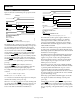


Table Of Contents
- FEATURES
- APPLICATIONS
- GENERAL DESCRIPTION
- FUNCTIONAL BLOCK DIAGRAM
- TABLE OF CONTENTS
- REVISION HISTORY
- SPECIFICATIONS
- ABSOLUTE MAXIMUM RATINGS
- PIN CONFIGURATION AND FUNCTION DESCRIPTIONS
- TYPICAL PERFORMANCE CHARACTERISTICS
- THEORY OF OPERATION
- OVERVIEW
- MODULATOR
- SLICER
- POWER STAGE
- GAIN
- PROTECTION CIRCUITS
- THERMAL PROTECTION
- OVERCURRENT PROTECTION
- UNDERVOLTAGE PROTECTION
- CLOCK LOSS DETECTION
- AUTOMATIC RECOVERY FROM PROTECTIONS
- MUTE AND STDN
- POWER-UP/POWER-DOWN SEQUENCE
- DC OFFSET AND POP NOISE
- SELECTING VALUES FOR CREF AND CIN
- MONO MODE
- POWER SUPPLY DECOUPLING
- EXTERNAL PROTECTION FOR PVDD > 15 V
- CLOCK
- APPLICATIONS INFORMATION
- OUTLINE DIMENSIONS

ADAU1592
Rev. A | Page 16 of 24
06749-043
V
CM
SLICER_LEVEL
50kΩ
V
TH
PIN 24 (SLC_TH)
R
EXTERNAL
Figure 43. Block for Slicer Threshold Adjust, SLC_TH
The slicer threshold can be set externally using a resistor as
follows:
⎟
⎟
⎠
⎞
⎜
⎜
⎝
⎛
+Ω
Ω
×
⎟
⎠
⎞
⎜
⎝
⎛
=
EXTERNAL
TH
R
AVDD
V
k50
k50
2
where:
AV D D = 3.3 V typical.
V
TH
is the voltage threshold at which the slicer is activated.
The following equation can be used to calculate the input signal
at which the slicer becomes active:
0.91.414
×
=
TH
IN rms
V
V
Therefore, for AV D D = 3.3 V typical and V
TH
= 1.1 V,
R
EXTERNAL
= 24.9 k
V
IN rms
= 0.864 V
Thus, the slicer is activated at and above 0.864 V
IN rms
.
This feature allows the user to set the slicer and, in turn, reduces
the output power at a given supply voltage. To disable the slicer,
SLC_TH should be connected directly to AGND.
Tabl e 9 shows
the typical values for R
EXTERNAL
.
Table 9. Typical R
EXTERNAL
Values
V
TH
(V) R
EXTERNAL
(kΩ) V
IN rms
(V)
1.1 24.9 0.864
1.17 20.5 0.919
1.24 16.5 0.974
1.32 12.4 1.037
POWER STAGE
The ADAU1592 power stage comprises a high-side PMOS and
a low-side NMOS. The typical R
DS-ON
is ~300 m. The PMOS-
NMOS stage does not need an external bootstrap capacitor and
simplifies the high-side driver design. The power stage also has
comprehensive protection circuits to detect the faults in typical
applications. See the
Protection Circuits section for further details.
GAIN
The gain of the amplifier is set internally using feedback
resistors optimized for 15 V nominal operation. The typical
gain values are tabulated in
Tabl e 1. The typical gain is 19 dB
with PGA set to 0 dB. PGA0 (Pin 14) and PGA1 (Pin 13) are used
for setting the desired gain.
The gain can be set according to
Tabl e 10. Note that the ampli-
fier full-scale input level changes as per the PGA gain setting.
Table 10. Gain Settings
PGA1
(Pin 13)
PGA0
(Pin 14)
PGA
Gain (dB)
Amplifier
Gain (dB)
Full-Scale
Input Level
(V
rms
)
0 0 0 19 1
0 1 6 25 0.5
1 0 12 31 0.25
1 1 18 37 0.125
PROTECTION CIRCUITS
The ADAU1592 includes comprehensive protection circuits. It
includes thermal warning, thermal overheat, and overcurrent or
short-circuit protection on the outputs. The
ERR
and
OTW
outputs are open-drain and require external pull-up resistors.
The outputs are capable of sinking 10 mA. The open-drain
outputs are useful in multichannel applications where more
than one ADAU1592 is used. The error outputs of multiple
ADAU1592s can be OR’ed to simplify the system design. The
logic outputs of the error flags ease the system design of using
a microcontroller.
THERMAL PROTECTION
Thermal protection in the ADAU1592 is categorized into two
error flags: one as thermal warning and the other as thermal
shutdown. When the device junction temperature reaches near
135°C (±5°C), the ADAU1592 outputs a thermal warning error
flag by pulling
OTW
(Pin 10) low. This flag can be used by the
microcontroller in the system for indication to the user or can
be used to lower the input level to the amplifier to prevent
thermal shutdown. The device continues operation until
shutdown temperature is reached.
When the device junction temperature exceeds 150°C, the
device outputs an error flag by pulling
ERR
(Pin 9) low. This
error flag is latched. To restore the operation,
MUTE
(Pin 15)
needs to be toggled to low and then to high again.
OVERCURRENT PROTECTION
The overcurrent protection in the ADAU1592 is set internally
at a 5 A peak output current. The device protects the output
devices against excessive output current by pulling
ERR
(Pin 9)
low. This error flag is latched. To restore the normal operation,
MUTE
(Pin 15) needs to be toggled to low and then to high
again. The error flag is useful for the microcontroller in the
system to indicate abnormal operation and to initiate the audio
MUTE
sequence. The device senses the short-circuit condition