
Specifications


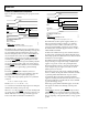


Table Of Contents
- FEATURES
- APPLICATIONS
- GENERAL DESCRIPTION
- FUNCTIONAL BLOCK DIAGRAM
- TABLE OF CONTENTS
- REVISION HISTORY
- SPECIFICATIONS
- ABSOLUTE MAXIMUM RATINGS
- PIN CONFIGURATION AND FUNCTION DESCRIPTIONS
- TYPICAL PERFORMANCE CHARACTERISTICS
- THEORY OF OPERATION
- OVERVIEW
- MODULATOR
- SLICER
- POWER STAGE
- GAIN
- PROTECTION CIRCUITS
- THERMAL PROTECTION
- OVERCURRENT PROTECTION
- UNDERVOLTAGE PROTECTION
- CLOCK LOSS DETECTION
- AUTOMATIC RECOVERY FROM PROTECTIONS
- MUTE AND STDN
- POWER-UP/POWER-DOWN SEQUENCE
- DC OFFSET AND POP NOISE
- SELECTING VALUES FOR CREF AND CIN
- MONO MODE
- POWER SUPPLY DECOUPLING
- EXTERNAL PROTECTION FOR PVDD > 15 V
- CLOCK
- APPLICATIONS INFORMATION
- OUTLINE DIMENSIONS

ADAU1592
Rev. A | Page 18 of 24
POWER-UP/POWER-DOWN SEQUENCE
Figure 46 shows the recommended power-up sequence for the
ADAU1592.
06749-046
AVDD/DVDD
PVDD
STDN
MUTE
OUTx+/OUTx–
PVDD/2
AINx
AVDD/2
t
PDL-H
t
INT
t
WAIT
t
INT
= 650ms @ 24.576MHz CLOCK
t
PDL-H
= 200µs
t
WAIT
= 10 × R
IN
× C
IN
INTERNAL MUTE
NOTES
1. INTERNAL MUTE IS INTERNAL TO CHIP.
Figure 46. Recommended Power-Up Sequence
The ADAU1592 has a special power-up sequence that consists
of a fixed internal mute time during which the power stage does
not start switching. This internal mute time depends on the
master clock frequency and is 650 ms for a 24.576 MHz clock.
Also, the internal mute overrides the external
MUTE
and
ensures that the power stage does not switch on immediately
even if the external
MUTE
signal is pulled high in less than
650 ms after
STDN
. The power stage starts switching only after
650 ms plus a small propagation delay of 200 µs have elapsed
and after
MUTE
is deasserted. Therefore, it is recommended to
ensure that t
WA I T
> t
INT
to prevent the pop and click during
power-up.
Ensure that the
MUTE
signal is delayed by at least t
WA I T
seconds after
STDN
. This time is approximately 10 times the
charging time constant of the input coupling capacitor.
For example, if the input coupling capacitor is 4.7 µF, the time
constant is
T = R × C = 20 kΩ × 4.7 µF = 94 ms
Therefore, t
WA IT
= 10 × T = 940 ms ~ 1 sec.
t
WA I T
is needed to ensure that the input capacitors are charged to
AVDD/2 before turning on the power stage.
When t
WA I T
< t
INT
, the power stage does not start switching until
650 ms have elapsed after
STDN
(see Figure 47). However, note
that this method does not ensure pop-and-click suppression
because of less than recommended or insufficient t
WA I T
.
t
INT
= 650ms @ 24.576MHz CLOCK
t
WAIT
<
t
INT
06749-047
A
VDD/DVDD
PVDD
S
TDN
MUTE
OUTx+/OUTx–
PVDD/2
A
INx
AVDD/2
t
INT
t
WAIT
INTERNAL MUTE
NOTES
1. INTERNAL MUTE IS INTERNAL TO CHIP.
Figure 47. Power-Up Sequence, t
WAIT
< t
INT
The ADAU1592 uses three separate supplies: AVDD (3.3 V
analog for PGA and modulator), DVDD (3.3 V digital for
control logic and clock oscillator), and PVDD (9 V to 18 V
power stage and level shifter). Separate pins are provided for
the AVDD, DVDD, and PVDD supply connections, as well as
AGND, DGND, and PGND.
In addition, the ADAU1592 incorporates a built-in undervolt-
age lockout logic on DVDD as well as PVDD. This helps detect
undervoltage operation and eliminates the need to have an external
mechanism to sense the supplies.
The ADAU1592 monitors the DVDD and PVDD supply voltages
and prevents the power stage from turning on if either of the
supplies is not present or is below the operating threshold.
Therefore, if DVDD is missing or below the operating thresh-
old, for example, the power stage does not turn on, even if
PVDD is present, or vice versa.
Because this protection is only present on DVDD and PVDD
and not on AVDD, shorting both AVDD and DVDD externally
or generating AVDD and DVDD from one power source is
recommended. This ensures that both AVDD and DVDD
supplies are tracking each other and avoids the need to monitor
the sequence with respect to PVDD. This also ensures minimal
pop and click during power-up.
When using separate AVDD and DVDD supplies, ensure that
both supplies are stable before unmuting or turning on the
power stage.
Similarly, during shutdown, pulling
MUTE
to logic low before
pulling
STDN
down is recommended. However, where a fault
event occurs, the power stage shuts down to protect the part. In
this case, depending on the signal level, there is some pop at the
speaker.