
Specifications


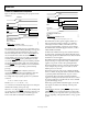


Table Of Contents
- FEATURES
- APPLICATIONS
- GENERAL DESCRIPTION
- FUNCTIONAL BLOCK DIAGRAM
- TABLE OF CONTENTS
- REVISION HISTORY
- SPECIFICATIONS
- ABSOLUTE MAXIMUM RATINGS
- PIN CONFIGURATION AND FUNCTION DESCRIPTIONS
- TYPICAL PERFORMANCE CHARACTERISTICS
- THEORY OF OPERATION
- OVERVIEW
- MODULATOR
- SLICER
- POWER STAGE
- GAIN
- PROTECTION CIRCUITS
- THERMAL PROTECTION
- OVERCURRENT PROTECTION
- UNDERVOLTAGE PROTECTION
- CLOCK LOSS DETECTION
- AUTOMATIC RECOVERY FROM PROTECTIONS
- MUTE AND STDN
- POWER-UP/POWER-DOWN SEQUENCE
- DC OFFSET AND POP NOISE
- SELECTING VALUES FOR CREF AND CIN
- MONO MODE
- POWER SUPPLY DECOUPLING
- EXTERNAL PROTECTION FOR PVDD > 15 V
- CLOCK
- APPLICATIONS INFORMATION
- OUTLINE DIMENSIONS

ADAU1592
Rev. A | Page 19 of 24
To shut down the power supplies to save power, it is highly
recommended to mute the amplifier before shutting down any
of the supplies. To achieve this, first pull down
MUTE
, then
shut down the power supplies in the following order: PVDD,
DVDD, and then AVDD. Where AVDD and DVDD are
generated from a single source, shut down PVDD before
shutting down DVDD and AVDD, and after issuing
MUTE
.
DC OFFSET AND POP NOISE
This section describes the cause of dc offset and pop noise
during turn-on/turn-off. The turn-on/turn-off pop in amplifiers
depends mainly on the dc offset, therefore, care must be taken
to reduce the dc offset at the output.
The first stage of the ADAU1592 has an inverting PGA amplifier,
as shown in
Figure 48.
0
6749-048
CHANGES WITH PGA SETTING
R
FB
TO NEXT STAGE
AINx
V
REF
C
REF
R
IN
R
SOURCE
V
MIS
C
IN
Figure 48. Input Equivalent Circuit
where:
R
IN
= 20 k, fixed internally.
R
FB
is the gain feedback resistor (value depends on the PGA
setting).
R
SOURCE
is the source resistance.
C
IN
is the input coupling capacitor (2.2 µF typical).
C
REF
is the filter capacitor for V
REF
.
V
REF
is the analog reference voltage (AVDD/2 typical).
V
MIS
is the dc offset due to mismatch in the op amp.
As shown in
Figure 48, the dc offset at the output can be due to
V
MIS
(the dc offset from mismatch in the op amp) and due to
leakage current of the C
IN
capacitor.
Normally, the offset due to leakage current in the C
IN
is less and
can be ignored compared to V
MIS
. The V
MIS
is mainly responsi-
ble for the dc offset at the output. The ADAU1592 uses special
self-calibration or a dc offset trim circuit, which controls the dc
offset (due to V
MIS
) to within ±3 mV. The V
MIS
can vary for each
part as well as for voltage and temperature. The trim circuit
ensures that the offset is limited within specified limits and
provides virtually pop-free operation every time the part is
turned on. However, care must be taken while unmuting or
during the power-up sequence.
During the initial power-up, C
IN
and C
REF
are charging to
AVDD/2 and, during this time, there can be dc offset at the
output (see
Figure 48). This depends on the PGA gain setting.
The dc offset is multiplied by the PGA gain setting. If the
amplifier is kept in mute during this charging and self-trimming
event for the recommended t
WA I T
time, the dc offset at the
output remains within ±3 mV. For more details on t
WA I T
, refer to
the
Power-Up/Power-Down Sequence section.
The amount of pop at the turn-on depends on t
WA I T
, which in
turn depends on the values of C
REF
and C
IN
. The following
section describes how to select the value for the C
REF
and C
IN
.
SELECTING VALUES FOR C
REF
AND C
IN
C
REF
is the capacitor used for filtering the noise from AVDD on
V
REF
. V
REF
is used for the biasing of the internal analog amplifier
as well as the modulator. Therefore, care must be taken to ensure
that the recommended minimum value is used. The minimum
recommended value for C
REF
is 4.7 µF.
C
IN
is the input coupling capacitor and is used to decouple the
inputs from the external dc. The C
IN
value determines the low
corner frequency of the amplifier. It can be determined from
the following equation:
ININ
LOW
CR
f
××π×
=
2
1
where:
f
LOW
is the low corner frequency (−3 dB).
R
IN
is the input resistance (20 k).
C
IN
is the input coupling capacitor.
Note that R
IN
= 20 k and R
SOURCE
< 1 k. If R
SOURCE
is sizable
with respect to R
IN
, it also must be taken into account in
calculation.
From the preceding equation, f
LOW
can be found for the desired
frequency response.
The recommended value for C
IN
is 2.2 µF, giving f
LOW
= 3.6 Hz,
and should keep 20 Hz roll-off within −0.5 dB.
However, if a higher than recommended C
IN
value is used for
better low frequency response, care must be taken to ensure that
appropriate t
WA I T
is used. See the Power-Up/Power-Down
Sequence
section for more details.
MONO MODE
The ADAU1592 mono mode can be enabled by pulling MO/
ST
(Pin 11) to logic high. In this mode, the left channel input and
modulator are active and feed PWM data to both the left and
right power stages. However, the respective power FETs need to
be connected externally for higher current capability. That is,
connect OUTL+ with OUTR+ and OUTL− with OUTR−. The
mono mode gives the capability to drive lower impedance loads
without invoking current limit. However, the output power is
limited by PVDD and temperature limits. See the typical applica-
tion schematic in
Figure 50 for details.
POWER SUPPLY DECOUPLING
Because Class-D amplifiers utilize high frequency switching,
care must be taken for power supply decoupling.
For reliable operation, using 100 nF ceramic surface-mount
capacitors for the PVDD and PGND pins is recommended. A
minimum of two capacitors is needed: one between Pin 45/Pin 46
(PVDD) and Pin 47/Pin48 (PGND), the other between Pin 39/
Pin 40 (PVDD) and Pin 37/Pin 38 (PGND). In addition, these