
Specifications

www.ti.com
TLV320AIC34
SLAS538A – OCTOBER 2007 – REVISED NOVEMBER 2007
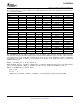
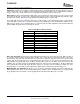
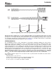
The following table lists several example cases of typical MCLK rates and how to program the PLL to achieve
f
S(ref)
= 44.1 kHz or 48 kHz.
f
S(ref)
= 44.1 kHz
MCLK (MHz) P R J D ACHIEVED f
S(ref)
% ERROR
2.8224 1 1 32 0 44100.00 0.0000
5.6448 1 1 16 0 44100.00 0.0000
12.0 1 1 7 5264 44100.00 0.0000
13.0 1 1 6 9474 44099.71 – 0.0007
16.0 1 1 5 6448 44100.00 0.0000
19.2 1 1 4 7040 44100.00 0.0000
19.68 1 1 4 5893 44100.30 0.0007
48.0 4 1 7 5264 44100.00 0.0000
f
S(ref)
= 48 kHz
MCLK (MHz) P R J D ACHIEVED f
S(ref)
% ERROR
2.048 1 1 48 0 48000.00 0.0000
3.072 1 1 32 0 48000.00 0.0000
4.096 1 1 24 0 48000.00 0.0000
6.144 1 1 16 0 48000.00 0.0000
8.192 1 1 12 0 48000.00 0.0000
12.0 1 1 8 1920 48000.00 0.0000
13.0 1 1 7 5618 47999.71 – 0.0006
16.0 1 1 6 1440 48000.00 0.0000
19.2 1 1 5 1200 48000.00 0.0000
19.68 1 1 4 9951 47999.79 – 0.0004
48.0 4 1 8 1920 48000.00 0.0000
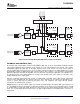
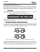
The TLV320AIC34 can also output a separate clock on the GPIO1_x pin. If the PLL is being used for the audio
data converter clock, the M and N settings can be used to provide a divided version of the PLL output. If the PLL
is not being used for the audio data converter clock, the PLL can still be enabled to provide a completely
independent clock output on GPIO1_x. The formula for the GPIO1 clock output when PLL is enabled and
CLKMUX_OUT is 0 is:
GPIO1_x = (PLLCLK_IN × 2 × K × R) / (M × N × P)
When CLKMUX_OUT is 1, regardless of whether PLL is enabled or disabled, the input to the clock output divider
can be selected as MCLK_x, BCLK_x, or GPIO2_x. Is this case, the formula for the GPIO1_x clock is:
GPIO1_x = (CLKDIV_IN × 2) / (M × N), where
M = 1, 2, 4, 8
N = 2, 3, … , 17
CLKDIV_IN can be BCLK_x, MCLK_x, or GPIO2_x, selected by page 0, register 102, bits D7 – D6
Copyright © 2007, Texas Instruments Incorporated Submit Documentation Feedback 33
Product Folder Link(s): TLV320AIC34