
Datasheet

TLV320AIC3107
SLOS545D –NOVEMBER 2008 –REVISED DECEMBER 2014
www.ti.com
Feature Description (continued)
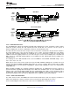
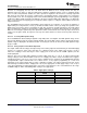
Table 1. Audio Clock Generation (continued)
Fsref = 44.1 kHz
3.072 1 1 32 0 48000.00 0.0000
4.096 1 1 24 0 48000.00 0.0000
6.144 1 1 16 0 48000.00 0.0000
8.192 1 1 12 0 48000.00 0.0000
12.0 1 1 8 1920 48000.00 0.0000
13.0 1 1 7 5618 47999.71 –0.0006
16.0 1 1 6 1440 48000.00 0.0000
19.2 1 1 5 1200 48000.00 0.0000
19.68 1 1 4 9951 47999.79 –0.0004
48.0 4 1 8 1920 48000.00 0.0000
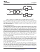
The TLV320AIC3107 can also output a separate clock on the GPIO1 pin. If the PLL is being used for the audio
data converter clock, the M and N settings can be used to provide a divided version of the PLL output. If the PLL
is not being used for the audio data converter clock, the PLL can still be enabled to provide a completely
independent clock output on GPIO1. The formula for the GPIO1 clock output when PLL is enabled and
CLKMUX_OUT is 0 is:
GPIO1 = (PLLCLK_IN× 2 × K × R) / (M × N × P) (3)
When CLKMUX_OUT is 1, regardless of whether PLL is enabled or disabled, the input to the clock output divider
can be selected as MCLK or BCLK. Is this case, the formula for the GPIO1 clock is:
GPIO1 = (CLKDIV_IN × 2) / (M × N)
where
• M = 1, 2, 4, 8
• N = 2, 3, …, 17
• CLKDIV_IN can be BCLK or MCLK, selected by page 0, register 102, bits D7-D6 (4)
10.3.3.2 Stereo Audio ADC
The TLV320AIC3107 includes a stereo audio ADC, which uses a delta-sigma modulator with 128-times
oversampling in single-rate mode, followed by a digital decimation filter. The ADC supports sampling rates from 8
kHz to 48 kHz in single-rate mode, and up to 96 kHz in dual-rate mode. Whenever the ADC or DAC is in
operation, the device requires an audio master clock be provided and appropriate audio clock generation be
setup within the part.
In order to provide optimal system power dissipation, the stereo ADC can be powered one channel at a time, to
support the case where only mono record capability is required. In addition, both channels can be fully powered
or entirely powered down.
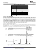
The integrated digital decimation filter removes high-frequency content and downsamples the audio data from an
initial sampling rate of 128 Fs to the final output sampling rate of Fs. The decimation filter provides a linear phase
output response with a group delay of 17/Fs. The –3 dB bandwidth of the decimation filter extends to 0.45 Fs
and scales with the sample rate (Fs). The filter has minimum 75dB attenuation over the stopband from 0.55 Fs to
64 Fs. Independent digital highpass filters are also included with each ADC channel, with a corner frequency that
can be independently set to three different settings or can be disabled entirely.
Because of the oversampling nature of the audio ADC and the integrated digital decimation filtering,
requirements for analog anti-aliasing filtering are relaxed. The TLV320AIC3107 integrates a second order analog
anti-aliasing filter with 20 dB attenuation at 1 MHz. This filter, combined with the digital decimation filter, provides
sufficient anti-aliasing filtering without requiring additional external components.
The ADC is preceded by a programmable gain amplifier (PGA), which allows analog gain control from 0 dB to
59.5 dB in steps of 0.5 dB. The PGA gain changes are implemented with an internal soft-stepping algorithm that
only changes the actual volume level by one 0.5 dB step every one or two ADC output samples, depending on
the register programming (see registers Page-0/Reg-19 and 22). This soft-stepping ensures that volume control
changes occur smoothly with no audible artifacts. On reset, the PGA gain defaults to a mute condition, and upon
24 Submit Documentation Feedback Copyright © 2008–2014, Texas Instruments Incorporated
Product Folder Links: TLV320AIC3107