
Datasheet

TLV320AIC3107
SLOS545D –NOVEMBER 2008 –REVISED DECEMBER 2014
www.ti.com
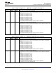
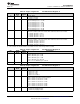
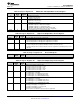
Table 29. Page 0 / Register 23: LINE2R to Right ADC Control Register
BIT READ/ RESET DESCRIPTION
WRITE VALUE
D7 R/W 0 LINE2R Single-Ended vs Fully Differential Control
If LINE2R is selected to both left and right ADC channels, both connections must use the same
configuration (single-ended or fully differential mode).
0: LINE2R is configured in single-ended mode
1: LINE2R is configured in fully differential mode
D6–D3 R/W 1111 LINE2R Input Level Control for Right ADC PGA Mix
0000: Input level control gain = 0.0 dB
0001-0011: Reserved. Do not write these sequences to these register bits
0100: Input level control gain = –6.0 dB
0101-0111: Reserved. Do not write these sequences to these register bits
1000: Input level control gain = –12.0 dB
1001-1110: Reserved. Do not write these sequences to these register bits
1111: LINE2R is not connected to the right ADC PGA
D2 R/W 0 Right ADC Channel Weak Common-Mode Bias Control
0: Right ADC channel unselected inputs are not biased weakly to the ADC common-mode voltage
1: Right ADC channel unselected inputs are biased weakly to the ADC common- mode voltage
D1–D0 R 00 Reserved. Write only zeros to these register bits
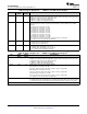
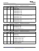
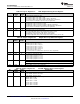
Table 30. Page 0 / Register 24: LINE1L to Right ADC Control Register
BIT READ/ RESET DESCRIPTION
WRITE VALUE
D7 R/W 0 LINE1L Single-Ended vs Fully Differential Control
If LINE1L is selected to both left and right ADC channels, both connections must use the same
configuration (single-ended or fully differential mode).
0: LINE1L is configured in single-ended mode
1: LINE1L is configured in fully differential mode
D6–D3 R/W 1111 LINE1L Input Level Control for Right ADC PGA Mix
Setting the input level control to a gain below automatically connects LINE1L to the right ADC
PGA mix
0000: Input level control gain = 0.0 dB
0001: Input level control gain = –1.5 dB
0010: Input level control gain = –3.0 dB
0011: Input level control gain = –4.5 dB
0100: Input level control gain = –6.0 dB
0101: Input level control gain = –7.5 dB
0110: Input level control gain = –9.0 dB
0111: Input level control gain = –10.5 dB
1000: Input level control gain = –12.0 dB
1001–1110: Reserved. Do not write these sequences to these register bits
1111: LINE1L is not connected to the right ADC PGA
D2–D0 R 000 Reserved. Write only zeros to these register bits.
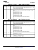
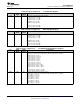
Table 31. Page 0 / Register 25: MICBIAS Control Register
BIT READ/ RESET DESCRIPTION
WRITE VALUE
D7–D6 R/W 00 MICBIAS Level Control
00: MICBIAS output is powered down
01: MICBIAS output is powered to 2.0V
10: MICBIAS output is powered to 2.5V
11: MICBIAS output is connected to AVDD
D5–D0 R/W 000000 Reserved. Write only zeros to these register bits.
54 Submit Documentation Feedback Copyright © 2008–2014, Texas Instruments Incorporated
Product Folder Links: TLV320AIC3107