
Datasheet

TLV320AIC3107
SLOS545D –NOVEMBER 2008 –REVISED DECEMBER 2014
www.ti.com
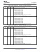
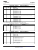
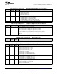
Table 47. Page 0 / Register 41: DAC Output Switching Control Register
BIT READ/ RESET DESCRIPTION
WRITE VALUE
D7–D6 R/W 00 Left DAC Output Switching Control
00: Left DAC output selects DAC_L1 path
01: Left DAC output selects DAC_L3 path to left line output driver
10: Left DAC output selects DAC_L2 path to left high power output drivers
11: Reserved. Do not write this sequence to these register bits.
D5–D4 R/W 00 Right DAC Output Switching Control
00: Right DAC output selects DAC_R1 path
01: Right DAC output selects DAC_R3 path to right line output driver
10: Right DAC output selects DAC_R2 path to right high power output drivers
11: Reserved. Do not write this sequence to these register bits.
D3–D2 R/W 00 Reserved. Write only zeros to these bits.
D1–D0 R/W 00 DAC Digital Volume Control Functionality
00: Left and right DAC channels have independent volume controls
01: Left DAC volume follows the right channel control register
10: Right DAC volume follows the left channel control register
11: Left and right DAC channels have independent volume controls (same as 00)
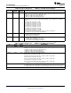
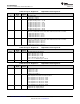
Table 48. Page 0 / Register 42: Output Driver Pop Reduction Register
BIT READ/ RESET DESCRIPTION
WRITE VALUE
D7-D5 R/W 000 Output Driver Power-On Delay Control
000: Driver power-on time = 0-μsec
001: Driver power-on time = 100-μsec
010: Driver power-on time = 10-msec
011: Driver power-on time = 100-msec
100: Driver power-on time = 400-msec
101: Driver power-on time = 2-sec
110–111: Reserved. Do not write these sequences to these register bits.
D4 R/W 0 Reserved. Write only zero to this register bit.
D3-D2 R/W 00 Driver Ramp-up Step Timing Control
00: Driver ramp-up step time = 0-msec
01: Driver ramp-up step time = 1-msec
10: Driver ramp-up step time = 2-msec
11: Driver ramp-up step time = 4-msec
D1 R/W 0 Weak Output Common-mode Voltage Control
0: Weakly driven output common-mode voltage is generated from resistor divider off the AVDD supply
1: Weakly driven output common-mode voltage is generated from bandgap reference
D0 R/W 0 Reserved. Write only zero to this register bit.
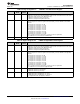
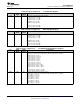
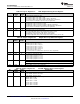
Table 49. Page 0 / Register 43: Left DAC Digital Volume Control Register
BIT READ/ RESET DESCRIPTION
WRITE VALUE
D7 R/W 1 Left DAC Digital Mute
0: The left DAC channel is not muted
1: The left DAC channel is muted
D6–D0 R/W 0000000 Left DAC Digital Volume Control Setting
0000000: Gain = 0.0 dB
0000001: Gain = –0.5 dB
0000010: Gain = –1.0 dB
…
1111101: Gain = –62.5 dB
1111110: Gain = –63.0 dB
1111111: Gain = –63.5 dB
60 Submit Documentation Feedback Copyright © 2008–2014, Texas Instruments Incorporated
Product Folder Links: TLV320AIC3107