
Data Sheet


19
FORM NO.: FR2-015_ A Responsible Department:WBU Expiry Date: Forever
The information contained herein is the exclusive property of AzureWave and shall not be distributed, reproduced, or disclosed
in whole or in part without prior written permission of AzureWave.
t
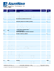
IH
Input Hold Time
Normal
5
-
High Speed
2
-
t
ODLY
Output Delay Time
Normal
-
14
High Speed
-
14
T
OH
Output hold time
High Speed
2.5
1. For SDIO 2.0 running at 50MHz clock frequency, only 1.8V is supported.
2. For SDIO 2.0 running at 25MHz clock frequency, 1.8V or 3.3V is supported.
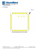
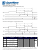
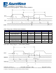
SDIO Protocol Timing Diagram – SDR12, SDR25, SDR50 Modes (up to 100MHz) (1.8V)
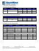
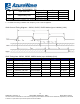
SDIO Timing Data- SDR12, SDR25, SDR50 Modes (up to 100MHz) (1.8V)
Symbol
Parameter
Condition
Min
Typ
Max
Units
f
pp
CLK Frequency
SDR12/25/50
25
-
100
MHz
T
IS
Input setup time
SDR12/25/50
3
-
-
ns
T
IH
Input hold time
SDR12/25/50
0.8
-
-
ns
T
CLK
Clock time
SDR12/25/50
10
-
40
ns
T
CR
, T
CF
Rise time, fall time
SDR12/25/50
-
-
0.2*T
CLK
ns
T
ODLY
Output delay time
SDR12/25/50
-
-
7.5
ns
T
OH
Output hold time
SDR12/25/50
1.5
-
-
ns