RS-485 Digital I/O Module Model 485SDD16 Document ation Number 485SDD16-1005 pn#3605-r1 This product Designed and Manufactured In Ottawa, Illinois USA of domestic and imported parts by B&B Electronics Mfg. Co. Inc. 707 Dayton Road -- P.O. Box 1040 -- Ottawa, IL 61350 PH (815) 433-5100 -- FAX (815) 433-5104 Internet: http://www.bb-elec.com sales@bb-elec.com support@bb-elec.
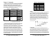
Table of Contents Chapter 5 - Software.............................................. 21 Programming Techniques..................................... 21 Read I/O Lines Command ..................................................21 Read Configuration Command ...........................................22 Set Output States Command ..............................................24 Define I/O Lines Command.................................................25 Set Power-up States Command ................................
Chapter 1- Introduction 485SDD16 Features The 485SDD16 is a general purpose control module that operates through an RS-485 interface. The 485SDD16 offers 16 discrete digital I/O lines. With these features, the module can be used to sense external ON/OFF conditions and to control a variety of devices. Each of the sixteen I/O lines can be defined as either an input or an output. The digital outputs are CMOS compatible. The digital inputs are CMOS/TTL compatible.
Power Supply Input Voltage: Connection: 8 Vdc to 16 Vdc @ 35 milliamps (Doesn’t include the power consumption of external devices.) Terminal Blocks or DB-25S Communications Standard: Addresses: Turn-around Delay: RS-422/485 256 (Factory default = 48 decimal) Software programmable from 0 to 255 character transmission times.
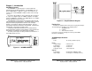
Serial Port Connections Chapter 2 - Connections This chapter will cover the connections required for the 485SDD16. There are three sets of connections: digital I/O, serial port, and power supply. Do not make any connections to the 485SDD16 until you have read this chapter. Digital I/O Connections Connections to the I/O lines are made through the DB25S (female) I/O port connector. Refer to Table 2.1. See Chapter 5 for I/O interfacing examples.
Figure 2.3 - RS-422 4-wire Connection Figure 2.1 - Example of Multi-Node Network Power Supply Connections 485SDD16 485SDD16 Power to the 485SDD16 must be supplied by an external power supply connected to the +12Vdc and GND terminal blocks or to the I/O connector. An external power supply must be able to supply 8 to 16 Vdc at 35ma. 485SDD16 NOTE: Power requirements of the module does not include the power consumption of any external devices connected to the module.
Table 3.2 - Equivalent Values Chapter 3 - Commands There are only two commands required to control the 485SDD16: set output lines, and read I/O lines. Five additional commands are used for configuring the module: set module address, set turnaround delay, define I/O lines, set power-up states, and read configuration. Command strings are from four to six bytes in length: the “!” character, an address byte, two command characters, and one or two data bytes (if required). (See Table 3.1). Table 3.
Read I/O Lines Command A byte represents an eight-bit binary number (11111111), therefore each byte can represent eight I/O lines. Each bit is assigned a bit position and a weight (value). Refer to Table 3.3. The Read I/O Lines command returns two data bytes that reflect the state of the I/O lines. The first data byte contains the most significant I/O lines (15 - 8). The second data byte contains the least significant I/O lines (7 - 0). If a bit is a "0" then the state of that I/O line is LOW.
Define I/O Lines Command Set Module Address Command The Set Module Address command is used to change the address of a 485SDD16. This commands requires one data byte. This data byte is used to specify the module's new address. Addresses can be assigned any decimal value from 0 to 255. The address is stored in non-volatile memory and is effective immediately. Each module must be assigned its own unique address when connected to an RS-485 muti-node network.
Set Power-up States Command The Set Power-up States command is used to set the states of output lines when the module's power is recycled. This command requires two data bytes. These data bytes specify the output state of each output line. The first data byte represents the eight most significant I/O lines (15 - 8). The second data byte represents the eight least significant I/O lines (7 - 0). If a bit position is set to a "0" then the state of that output line will be set LOW.
Chapter 4 - I/O Interfacing This chapter will explain "HIGH" and "LOW" states and show some general examples of how to interface to the I/O lines. Caution must be taken not to exceed 485SDD16 specifications listed in Chapter 1 when interfacing to external devices. Failure to stay within these specifications could result in damage to the unit and will void warranty. Digital Inputs As stated earlier, digital input lines are CMOS/TTL compatible and can only handle voltages from 0Vdc to +5Vdc.
Figure 4.4 - Isolated Solid State Input Figure 4.6 - Isolated Solid State Output Digital Outputs Digital outputs are used to turn on or turn off external devices. Digital outputs are CMOS compatible and operate between 0Vdc and +5Vdc. Outputs can be used to control solid state output modules, CMOS and TTL logic circuits. Caution must be taken not to exceed the power capability of the outputs. Refer to the output specifications in Chapter 1.
Chapter 5 - Software This chapter will be divided into two sections. The first section covers programming techniques for constructing a command string, receiving data and manipulating data in QuickBASIC. The second section discusses how to install and run the demonstration program on an IBM PC or compatible. Programming Techniques This section shows steps and examples of programming the 485SDD16 in QuickBasic.
Step 3 - Receiving the data: MSdefs$ = INPUT$(1,#1) LSdefs$ = INPUT$(1,#1) MSpups$ = INPUT$(1,#1) LSpups$ = INPUT$(1,#1) Maddr$ = INPUT$(1,#1) Mtdly$ = INPUT$(1,#1) Step 4 - Manipulating the data: MSdefs = ASC(MSdefs$) LSdefs = ASC(LSdefs$) MSpups = ASC(MSpups$) LSpups = ASC(LSpups$) Maddr = ASC(Maddr$) Mtdly = ASC(Mtdly$) Step 5 - Determining the I/O line definitions: MSdefs = MSdefs AND mask LSdefs = LSdefs AND mask By "ANDing" the value of MSdefs or LSdefs with the appropriate mask of an I/O line, the I/
Step 1b - Set appropriate outputs LOW MSstates = MSstates AND (NOT(mask)) LSstates = LSstates AND (NOT(mask)) By "ANDing" the current states with the complement of the appropriate mask of a digital output line, the output's bit will be set to a "0" (LOW). Step 1c - Completing the command string: Cmnd$ = "!" + CHR$(Maddr) + "SO" + CHR$(MSstates) + CHR$(LSstates) Step 2 - Transmitting the command string: Print #1, Cmnd$; Example 5.3 - Set Output #0 HIGH and Output #14 LOW of module #5. 'Set module address.
Step 1b - Set appropriate outputs power-up states LOW MSpups = MSpups AND (NOT(mask)) LSpups = LSpups AND (NOT(mask)) By "ANDing" the current power-up states with the complement of the appropriate mask of a digital output line, the power-up state's data bit will be set to a "0" (LOW). Step 1c - Completing the command string: Cmnd$ = "!" + CHR$(Maddr) + "SS" + CHR$(MSpups) + CHR$(LSpups) Step 2 - Transmitting the command string: Print #1, Cmnd$; Example 5.
Demonstration Program The 485SDD16 Demonstration (SDD16) Program (IBM PC or Compatible) provides the user with examples of how to receive and transmit commands to the 485SDD16. The SDD16.EXE is the executable program, the SDD16.BAS file is the source code in QuickBASIC. The source code provides an illustration of how to send and receive commands from the 485SDD16. NOTE: This is a demonstration program only and not intended for system applications.
Decimal ASCII 0 ................... NUL 1 ................... SOH 2 ................... STX 3 ................... ETX 4 ................... EOT 5 ................... ENQ 6 ................... ACK 7 ................... BEL 8 ................... BS 9 ................... HT 10 ................. LF 11 ................. VT 12 ................. FF 13 ................. CR 14 ................. SO 15 ................. SI 16 ................. DLE 17 ................. DC1 18 ................. DC2 19 .................
Decimal............ ASCII 80 ................. P 81 ................. Q 82 ................. R 83 ................. S 84 ................. T 85 ................. U 86 ................. V 87 ................. W 88 ................. X 89 ................. Y 90 ................. Z 91 ................. [ 92 ................. \ 93 ................. ] 94 ................. ^ 95 ................. _ 96 ................. ' 97 ................. a 98 ................. b 99 ................. c 100 ...............
The decimal (base 10) numbering system represents each position in successive powers of 10, with each decimal symbol having a value from 0 to 9. The hexadecimal (base 16) numbering system represents each position in successive powers of 16 with each hex symbol having a value of 0 to 15. Since each hex position must have a single symbol, the symbols "A" through "F" are assigned to values 10 through 15 respectively. Refer to Table 1.
Hexadecimal to Decimal Conversion: Decimal = (1st Hex digit x 4096) + (2nd Hex digit x 256) + (3rd Hex digit x 16) + (4th Hex digit) Each "Hex digit" is the decimal equivalent value of the hexadecimal symbol. Example: Convert 10FC hexadecimal to decimal. 1 x 4096 = 4096 0 x 256 = 0 15 x 16 = 240 12 x 1 = 12 4348 10FC hex equals 4348 decimal. Decimal to Hexadecimal Conversion: Example: Convert 4348 decimal to hexadecimal.
DTB25 The DTB25 connects to the SDD16 models to provide easy access to the available I/O lines. The DTB25 plugs directly into the SDD16's DB25S I/O port connector. Each of the twenty-five pins on the connector is brought out to a terminal block. Refer to Table C.1. Dimensions: 0.5" x 2.1" x 4.3". An enclosure for the DTB25 is available. APPENDIX C Interface Modules for SDD16 Models Figure C.
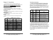
Table C.2 - DBM16 I/O Connections Table C.1 - DTB25 Connections DB-25P Pin # 1 2 3 4 5 6 7 8 9 10 11 12 13 Function T.B. # DB-25P Pin # Function T.B. # Unused. Unused. Unused. Unused. Unused. Unused. Ground +12Vdc Input I/O #0 I/O #1 I/O #2 I/O #3 I/O #4 1 2 3 4 5 6 7 8 9 10 11 12 13 14 15 16 17 18 19 20 21 22 23 24 25 I/O #15 I/O #14 I/O #13 I/O #12 I/O #11 I/O #10 Unused. I/O #9 I/O #8 I/O #7 I/O #6 I/O #5 14 15 16 17 18 19 20 21 22 23 24 25 T.B.
Figure C.4 - Solid State Input Figure C.2 - DBM16 Outline Drawing Inputs Digital inputs are used to sense "HIGH" and "LOW" states based on voltage levels. This is accomplished via switch closures, contact closures or a solid state digital signals. Each DBM16 input is pulled up through a resistor and will be read as a logic "1" (HIGH) by the SDD16 module. When an input on the DBM16 is grounded (below +1.5Vdc), a logic "0" (LOW) will be read by the SDD16 module. Figures C.3 - C.
Outputs Digital outputs are used to turn "ON" or turn "OFF" external devices. Outputs can be used to control solid state output modules, logic circuits, and relays. Caution must be taken not to exceed the power capability of the outputs. Refer to the DBM16 output specifications. Setting the SDD16 module's output line to a "1" turns "ON" the DBM16's output line. Setting the SDD16 module's output line to a "0" turns "OFF" the DBM16's output driver. The DBM16 outputs are open collector current sinking drivers.
Figure C.
With serial communications in a laboratory environment, the possibility of a communication error occurring is minimal. However, in a harsh or an industrial environment the possibility increases. A communication error occurs when a bit transmitted as a “1” is received as a “0” or vice versa. If the 485SDD16 receives a error in one or more of the first four command characters (“!0xx”), the unit will not execute the command.
Table D-1 Extended Commands Function Command Response Read I/O Lines #{addr}RD Set Output Lines #{addr}SO{I/O msb}{~I/O msb}{I/O lsb}{~I/O lsb} #{addr}SA{new addr}{~new addr} #{addr}SC{x}{~x} {I/O msb}{~I/O msb}{I/O lsb}{~I/O lsb} no response Set Module Address Set Turn-around Delay Define I/O Lines Set Power-up States Read Configuration #{addr}SD{I/O msb}{~I/O msb}{I/O msb}{~I/O msb} #{addr}SS{I/O msb}{~I/O msb}{I/O lsb}{~I/O lsb} #{addr}RC no response no response no response no response {I/O