Not Recommended for New Installations. Please contact Technical Support for more information. Optically Isolated Serial Data Acquisition Module 232OPSDA Module Documentation Number 232OPSDA1397 This product Designed and Manufactured In Ottawa, Illinois USA of domestic and imported parts by B&B Electronics Mfg. Co. Inc. 707 Dayton Road -- P.O. Box 1040 -- Ottawa, IL 61350 PH (815) 433-5100 -- FAX (815) 433-5105 Internet: http://www.bb-elec.com orders@bb-elec.com support@bb.elec.
TABLE OF CONTENTS CHAPTER 1: INTRODUCTION ...........................................................1 232OPSDA FEATURES ...........................................................................1 PACKING LIST .........................................................................................2 SOFTWARE INSTALLATION ......................................................................3 232OPSDA SPECIFICATIONS ..................................................................
APPENDIX A: DEC TO HEX TO ASCII CONVERSION.......... A-27 APPENDIX B: 232OPSDA SCHEMATIC & BOARD .................
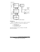
Chapter 1: Introduction 232OPSDA Features The 232OPSDA is an optically isolated data acquisition module that is connected to your computer’s RS-232 serial port. It provides 2500V of optical isolation protection between the I/O and RS-232 side of the module. The 232OPSDA offers six channels of 12-bit A/D, one digital input, and one digital output. The six A/D input channels can be used for a number of applications.
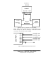
Terminal Blocks Digital Input TB 6 Digital Output Digital I/O TB 7 Microprocessor Optical Isolation Serial Port DB-25S TD A/D 3 A/D 2 A/D 5 A/D 0 TB 5 Analog Inputs A/D 4 A/D 1 A/D Converter TB 4 RD A/D 1 TB 2 A/D 2 TB 3 A/D 3 A/D 3 TB 1 A/D 2 A/D 0 A/D 0 TB 0 A/D 1 RS-232 Tranceiver Signal Conditioning Circuitry Figure 1.2: General Block Diagram Packing List Examine the shipping carton and the contents for physical damage.
Software Installation The 232OPSDA comes with several a demonstration program. To install these programs on your hard drive: 1. 2. 3. 4. Place the disk in drive A. Type A: and press the key. Type INSTALL and press the key. Follow the instructions given by the program. The file, READ.ME, contains corrections and additions to the printed user’s manual. The file, FILES.LST, contains a list and description of the files installed on the hard drive. The file, HISTORY.
Digital Input Channels: Voltage Range: Low Voltage: High Voltage: Leakage Current: 1 -30VDC to +30VDC -30VDC to 1.0VDC 2.0VDC to 30VDC 1 µA maximum Digital Output Channels: Low Voltage: High Voltage: 1 0.6VDC @ 8.7mA 4.3VDC @ -5.4mA Power Supply Input Voltage: Connections: 9-16VDC @ 10mA (Does not include the power consumption of external devices.
Chapter 2: Connections This chapter will cover the connections required for the 232OPSDA. Four sets of connections are required: A/D converter, digital I/O, serial port, and power supply connections. Do not make any connections until you have read this chapter. If you do not use a particular type of connection, it is still important to read each section. Table 2.1 shows the terminal block assignments. Table 2.
RS-232 Port GND A/D 5 TB 5 Output TB 8 A/D 4 TB 4 TB 3 A/D 3 A/D 2 TB 2 TB 0 TB 1 A/D 0 A/D 1 232OPSDA Input 4-20mA Current Loop Transmitter 4-20mA Current Loop Return Out 4-20mA Current Loop Receiver Figure 2.1: Current Loop Channel Connections (A/D 0) 232OPSDA NOTE: When using the 4-20mA Current Loop Input with the setup shown in Figure 2.1, A/D 1-5 cannot be used and should be connected to the terminal block labeled GND.
Digital I/O Connections The digital I/O connections are made on the I/O port, which consists of terminal blocks. Table 2.1 shows the terminal block assignments. Digital Input Terminal block 7 is the digital input line. This input is CMOS/TTL compatible and can handle voltage from -30VDC to 30VDC. If a digital input is from -30VDC to 1.0VDC, the state will be read as a “0” (LOW). If a digital input is from 2.0VDC to 30VDC, the state will be read as a “1” (HIGH).
Table 2.2 - RS-232 Connector Pinout DB25S Pin # 232OPSD A Function Signal 2 3 4 5 Transmit Data (TD) Receive Data (RD) Request to Send (RTS) Clear to Send (CTS) 6 Data Set Ready (DSR) 7 8 Signal Ground (SG) Data Carrier Detect (DCD) 12 20 Signal Ground (SG) Data Terminal Ready (DTR) Optional Power Supply Connection 25 Input Output Input Input Notes Connection is required. Connection is required. Used for power. Internally connected to RTS (pin 4). Internally connected to DTR (pin 20).
Power Supply Connections The 232OPSDA requires an isolated external power supply that is able to produce 9-16VDC @10mA in addition to the port power. The positive(+) lead of the power supply is connected to the terminal block labeled +12VDC and the negative(-) lead is connected to the terminal block labeled GND. The external power supply powers the I/O side of the module. The RS-232 side of the module is port powered using RTS and DTR. These lines may be either LOW or HIGH to provide power to the module.
Chapter 3: Commands Only three commands are required to operate the 232OPSDA: the read A/D command, read digital I/O command, and the set digital output command. The command string consists of four bytes. The read A/D and digital I/O commands require an additional data byte. See Table 3.1. Table 3.
Table 3.2 - Equivalent Values ASCII Decimal Hexadecimal ! # 0 A D O R S NUL SOH STX ETX EOT ENQ ACK BEL 33 35 48 65 68 79 82 83 0 1 2 3 4 5 6 7 21h 23h 30h 41h 44h 4Fh 52h 53h 0h 1h 2h 3h 4h 5h 6h 7h Syntax As mentioned earlier, the command string consists of four bytes. The first byte is the start of message byte. The start of message byte is always the “!” character. The second byte is the address byte. This byte allows each unit to have a unique address (useful in RS485 networks).
The command syntax for the extended command set is shown below: Command Syntax: # 0 _ _ _ _ | | | | | | | | | | | Compliment | | | | Data Byte | | | 2nd Command Byte | | 1st Command Byte | Address Byte Start of Message Byte Reading A/D Channels Command The Read A/D channels command returns two bytes for each channel read. The two bytes represent the most significant byte (MSB) and least significant byte (LSB) of the reading. The MSB is received first, followed by the LSB. This command requires a data byte.
Table 3.3 - Read A/D Response # of Channels Specified decimal Hex ASCII 0 1 2 3 4 5 0 1 2 3 4 5 NUL SOH STX ETX EOT ENQ Response Channels Returned (order of response) Channel 0 Channels 1,0 Channels 2,1,0 Channels 3,2,..,0 Channels 4,3,..,0 Channels 5,4,..,0 Bytes Returned 2 4 6 8 10 12 NOTE: There are three test channels that can be read: Ref+, Ref-, and Ref+/2. Specify 13 (0Dh) to read Ref+, 12 (0Ch) to read Ref-, and 11 (0Bh) to read Ref+/2.
Chapter 4: A/D This chapter will deal with the various A/D channels and manipulating the data obtained from them. Sampling Rate The A/D converter has a conversion time around 10 microseconds, however, the actual sampling rate is limited by the serial communications. The actual sampling rate for a single channel is around 120 samples per second (9600 baud). This rate drops to around 41 samples per second when sampling all of the channels.
inverting amplifier, remove R15 and calculate values for R13 and R14 using the equation below. Gain = V0 R13 = 1+ Vin R14 NOTE: V0 is the voltage read by the A/D converter chip, and Vin is the voltage at TB1. R13 and R14 should be chosen so that V0 does not exceed 5.00VDC. 0 to 10VDC A/D Input The 232OPSDA contains one A/D input than is capable of handling voltages between 0VDC and 10VDC. This channel is A/D 3 and is located on Terminal Block 3.
The signal conditioning circuit for this A/D input channel has been designed to be easily modified. In the original configuration, R5 and R6 are left OPEN (they are not present). These two spaces are provided if you need a different gain. Reducing the gain of this noninverting amplifier allows you to measure currents up to 100mA, and increasing the gain allows you to read much smaller currents with greater accuracy. See the circuit schematic in Figure B.1 and board layout in Figure B.2 in Appendix B.
Chapter 5: Software Application Program Interface The application program interface (API) is a set of routines that makes it easy to communicate with the 232OPSDA module from a 16bit DOS application. Example programs using the API are written in Borland C++, Borland Pascal and Microsoft® QuickBASIC v4.5. The batch file, MAKEIT.BAT, in the directory for each language shows how to compile and link the demo program with the API routines.
segment and offset addresses of the integer array where the results of the A/D conversion will be stored. Returns: FALSE (zero) if the function fails, otherwise it returns TRUE (non-zero). B232OPSDA_ReadDigital Purpose: This function reads the states of all the digital I/O lines.
B232OPSDA_SetDigitalOutput Purpose: This function sets the states of the digital output lines.
Syntax: Remarks: C: WORD initComPort (WORD portAddr, BYTE irq, LONG baudRate); Pascal: function initComPort (portAddr : word; irq : byte; baudRate : longint) as integer; BASIC: FUNCTION initComPort% (BYVAL portAddr AS INTEGER, BYVAL irq AS INTEGER, BYVAL baudRate AS INTEGER) portAddr is the address of the serial port. irq is the interrupt request number that the serial port uses. baudRate is the speed at which the API talkes to the 232OPSDA module.
‘ Open the serial port. ‘ OPEN “COM1:9600,N,8,1,cd,ds” FOR RANDOM AS #1 PAUSE (.5) ‘ Close the serial port when finished. ‘ CLOSE #1 Read A/D Command The read A/D channels command returns two bytes of data for each channel read. The two bytes represent the most significant byte (MSB) and least significant byte (LSB) of the reading. The MSB is received first, followed by the LSB. This command requires a data byte. The data byte is used to specify the number of the highest channel to be read.
Step 5 - Repeat Step 3 and 4 until each channel has been completed. Step 6 - The various A/D channels have signal conditioning, so mathematical manipulation of the voltage read will have to be performed. See Chapter 4 for the equations. Example 5.1 - Read A/D channels 1 and 0 gain0 = 23.
Step 1 - Constructing the command string: Command$ = “!0RD” Step 2 - Transmitting the command string: Print #1, Command$ Step 3 - Receiving the data: Reply$ = INPUT$ (1, #1) Step 4 - Manipulating the data: states = ASC(Reply$) Step 5 - Determining an I/O’s status status = states AND mask By “ANDing” the value of states with the appropriate mask of an I/O line, the status of can be determined. If status is equal to zero then the I/O line is LOW. If status is not equal to zero then the I/O line is HIGH.
Set Digital Output State The Set Digital Output command is used to set the state of the digital output line. This command requires a data byte. The data byte is used to specify the output state. Bit 0 corresponds to the state of digital output. If a bit is a 0 then the output will be set LOW. If a bit is a 1 then the output will be set HIGH. Note: This command ignores Bits 1-7 of the data byte.
Appendix A: Decimal to Hex to ASCII Conversion DECIMAL to HEX to ASCII CONVERSION TABLE DEC HEX ASCII KEY DEC HEX ASCII DEC HEX ASCII DEC HEX ASCII 0 0 NUL ctrl @ 32 20 SP 64 40 @ 96 60 ` 1 1 SOH ctrl A 33 21 ! 65 41 A 97 61 a 2 2 STX ctrl B 34 22 “ 66 42 B 98 62 b 3 3 ETX ctrl C 35 23 # 67 43 C 99 63 c 4 4 EOT ctrl D 36 24 $ 68 44 D 100 64 d 5 5 ENQ ctrl E 37 25 % 69 45 E 101 65 e 6 6 ACK ctrl F 38 26 & 70 46 F 102 66