CI270CW 533MHz FSB / VGA / DVI / Multi-COMs / LAN / Mini PCI / PCIe mini card Intel Atom N270 . 533MHz FSB . All-In-One . Audio . LAN . Mini PCI . PCIe mini card SATA . 8 USB . CF . Wide range DC-input Multi-COM Board NO. CI270CW Release date: OCT . 01 .
Contents CI270CW Warning!........................................................................................................................... 1 Hardware Notice Guide ............................................................................................. 2 CHAPTER 1 GENERAL INFORMATION ........................................................................ 4 1-1 MAJOR FEATURE........................................................................................................
-9 USB PORT .................................................................................................................. 33 3-10 LAN CONNECTOR ................................................................................................... 34 3-11 COM PORT CONNECTOR ....................................................................................... 35 3-12 AUDIO PORT CONNECTOR ....................................................................................
CHAPTER 5 DRIVER INSTALLATION........................................................................ 81 5-1 INF INSTALL INTEL 945GSE CHIPSET SYSTEM DRIVER .................................. 83 5-2 VGA INSTALL INTEL 945GSE VGA DRIVER ........................................................... 85 5-3 SOUND INSTALL VIA HID AUDIO CODEC DRIVER ............................................... 87 5-4 HOW TO UPDATE BIOS ............................................................................................
2009 OCT . 01.
Warning ! 1. Battery Battery on board is consumables. We doesn’t guarantee the life time of it. 2. Fanless solution with HDD Please be aware of specification & limitation for HDD when fanless solution is implemented. 3. We will not give further notification if there is any change about the product information and the manual. 4. SATA does not support Hot SWAP 5. There would be +-20% difference of WDT at room temperature. 6.
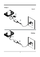
* Hardware Notice Guide 1. Before installing the power supply with this motherboard, please attach the 12V/DC ( 4 pin connector )of the adapter to motherboard first. After that, plug the adapter power to AC outlet. Always normally shut down the computer before you move the system unit or remove the power supply from the motherboard. Please unplug the 12V/DC ( 4 pin connector ) of the adapter from motherboard first. Then unplug the adapter from the AC outlet. Please refer to procedure from the photo 1 2.
Photo 1 Insert 1 2 3 Unplug 1 2 3 3
Chapter-1 General lnformation The CI270CW is an All-In-One POS / Automation control Board. The board's design combines all necessary input and output effects interfaces, which makes itself an ideal all-in-one control board for demanding POS or automation control applications. CI270CW is the perfect platform for a whole range of mobile and low-power devices.
1-1 Major Feature 1. Intel Atom N270 CPU ( FSB 533 Mhz ) 2. Intel 945GSE Chipset on board, Graphic Chip Integrated 3. On board DDR2 module 1GB and support DDR2 SODIMM up to 2GB (option) 4. On board SSD 1/2/4/8 Gbytes (option) 5. Support 2 x 10 / 100 / 1000 Mbps LAN on Board ( Realtek or Intel LAN Chip ) 6. Support CRT resolutions up to SXGA+ 7. 18 bits/ 36 bits LVDS Interface on Board. (option) 8. Support DVI. 9. Support 1 x Compact Flash Card Socket and 40 pin IDE socket on Board 10.
1-2 Specification 1. CPU: Intel Atom N270 CPU ( FSB 533 Mhz ) 2. ChipSet: Intel 945GSE and Intel ICH7M (82801GBM) 3. Memory: On board DDR2 module 1 GB or support DDR2 SODIMM up to 2GB 4. VGA: Internal Graphics Memory with dynamic video memory technology (DVMT3.0) 5. I/O Chip: ITE IT8712F and F81216AD IO chipset 6. SATA: Two SATA ports with independent DMA operation supported 7. NAND flash memory (option): Support Compact Flash card type II for ATA interface On board SSD 1/2/4/8 GBytes 8.
1-3 Vertical SODIMM assembly guide 1. Install the memory into SODIMM. 2. Press down firmly to ensure the memory is locked. Uninstall 1. Pull open both sides of the memory slot. 2. Take out the memory.
1-4 Directions for installing the Mini Card 1. Unscrew the screw on the board 2. Plug in the Mini Card in a 45 angle 3. Gently push down the Mini Card and screw the screw back.
1-5 Installing the Mini PCI card 1.Align the Mini PCI card with the connector at a 45 degree angle. 2. Press the Mini PCI into the connector until you hear a click. Notices: 2. Make sure the retaining clips (on two sides of the slot) 1.The connectors are designed to ensure the lock onto the notches of the card firmly correct insertion. If you feel resistance, check the connectors & golden finger direction, and realign the card. 1-5-1.1 Removing the Mini PCI card 1.
1-6 Packing List 1 5 3 2 6 4 7 1 MotherBoard 4 SATA HDD Cable(7P) 2 DC 12V Power Adapter(4P) 5 Power Cable 3 ATA 66 HDD Cable(40P) 6 Utility CD Disk 7 User’s Manual *The packing list above is for the users who purchase single motherboard. The users who purchase the board with chassis may refer to the packing list in the Assembly Guide. Please contact with your dealer if any of these items is missing or damaged on delivery.
Chapter-2 Hardware Installation This chapter provides the information how to install the hardware of CI270CW. Please follow section 1-6, 2-1 and 2-2 to check the delivery package and unpack carefully. Please follow the jumper setting procedure. 2-1 Unpacking Precaution The CI270CW board has been well packed with an anti-static bag to protect its sensitive components and circuitry from damage due to static electric discharge. NOTE! 1.
2-2 Unpacking checkup First of all, please follow all necessary steps of section 2-1 to protect CI270CW from electricity discharge. With reference to section 1-6, please check the delivery package again with following steps: 1. Unpack the CI270CW board and keep all packing material, manual and driver disc etc, do not dispose ! 2. Is there any components lose or drops from the board? DO NOT CONTINUE TO INSTALL THIS BOARD! CONTACT THE DEALER YOU PURCHASED THIS BOARD FROM, IMMEDIATELY. 3.
2-3 Dimension 200 x 150 mm 135.000 130.900 93.000 19.100 7.100 116.000 CI270C-M0.1 19.100 rj45 rj45 16.600 34.000 2009,02,25 9.5 25.48 5.100 53.44 84.68 105.56 13 6.5 6.28 22.16 22.6 13.02 4.22 5 6.79 7 19 21.59 20.88 132.65 168.71 191.
2-4 Layout - CI270CW SWP13 SODIM1 CPI1 FAN1 CFP2 JSP1 SWP1 SWP12 CFP1 LED1 CPI11 CKM11 CKM1 LED2 CG11 LVDS1 CDG1 CUL2 JSD1 JVL1 JVP1 CUL1 FAN2 CU7 LPT1 CC6 CC12 CC22 CC5 CC23 MPCE1 CC11 JVC1 CC21 JVC2 JSC3 CVO1 CPP1 SATA2 SATA1 CA3 JSB1 JSV1 CVO11 JSC31 CC34 JSC32JSC33 JSC34 CVI1 JVC3 JVC4 CA1 CA2 CU8 CU12 JUSB1 JUSB2 CA12 CAL1 CF1 CAR1 14 JSF1 CO1 CT1 JVF1 CIO1 CIO2 IDE1 JVU8 CPO1
2-5 Diagram - CI270CW CPI1 SWP13 FAN1 CFP2 SODIM1 JSP1 SWP1 SWP12 CFP1 CKM1 LED1 CG11 CDG1 LVDS1 CUL2 JSD1 JVL1 JVP1 CPP1 SATA2 CUL1 FAN2 CU7 LPT1 CC6 CC12 CC5 JVC1 MPCE1 CC21 JVC2 JSC3 SATA1 CA3 JSB1 CA1 JSC31 CC34 JSC32 JSC33 JSC34 CVI1 JVC3 JVC4 CA2 CU8 CU12 CA12 JSF1 CAL1 CAR1 CF1 15 CO1 CT1 JVF1 CIO2 CIO1 IDE1 JVU8 CPO1
2-5-1 Bottom Side Diagram- CI270CW MPCI: Mini PCI Socket Back Panel-CI270CW PS/2 Mouse VGA LAN 2 LAN 1 COM 1 COM 3 COM 2 COM 4 Line-out DC 12V IN PS/2 Keyboard DVI USB Front Panel-CI270CW USB Line-out phone jack Mic-in phone jack 16 Mic-in
2-6 Install Memory This motherboard provides one 200-pin Small Outline Dual In-line Memory Module (SODIMM) socket for memory expansion available from minimum memory size of 256MB to maximum memory size of 2GB DDR2 SDRAM. DDR2 clock supports: DDR2 533, DDR2 667 Valid Memory Configurations Total Memory DIMM1 System Accept or Not DS/SS Accept DS: Double Sided DIMM Min. ~ Max.
NOTE! When you install DIMM module fully into the DIMM socket, the eject tab should be locked into the DIMM module very firmly and fit into its indention on both sides. Please refer to page7 for installation of memory module. WARNING! Once you hear " Beep Beep Beep" sounds after turning on the power , please check if the DRAM is installed properly or not. 2-7 List of Jumpers 1. JSB1: CMOS clear select 2. JSC3, JSC31 / 32 / 33 / 34: COM3 RS232/422/RS485 select 3. JSP1: ATX / AT Power type select 4.
2-8 Jumper Setting Description A jumper is ON as a closed circuit with a plastic cap covering two pins. A jumper is OFF as an open circuit without the plastic cap. Some jumpers have three pins, labeled 1, 2, and 3. You could connect either pin 1 and 2 or 2 and 3. The below figure 2.2 shows the examples of different jumper settings in this manual. Figure 2.2 All jumpers already have its default setting with the plastic cap inserted as ON, or without the plastic cap as OFF.
Note: Do not clear CMOS unless 1. Troubleshooting 2. Forget password 3. You fail over-clocking system JSB1 *1-2 2-3 Description *Normal Set CMOS Data clear JSB1 3 2 1 3 2 1 *Normal Clear Setting 2-10 JVF1: CF Card Power Voltage select If you use CF card and HDD together, we suggest you use the jumper setup for +5V. *We strongly suggest the users: DO NOT use the CF Card & HDD at the same time. JVF1 Description *1-2 *For CF CARD power voltage select +5V 2-3 For CF CARD power voltage select +3.
2-11 JSF1: CF Card Master and Slave select If you use CF card and SSD together, please set CF as Slave and SSD as Master. *We strongly suggest the users: DO NOT use the SSD & CF Card at the same time.
2-13 COM port pin9 select RI signal or Voltage source JVC1: COM1 PIN9 select JVC3: COM3 PIN9 select JVC1 / 2 / 3 / 4 *1-2 JVC2: COM2 PIN9 select JVC4: COM4 PIN9 select Description *COM port pin9 use RI signal 3-4 COM port pin9 use +5V voltage 5-6 COM port pin9 use +12V voltage Note: 1. Please be cautious about voltage setting. 2. If want to use +5V/+12V need check system power design spec.
2-14 JSC3,JSC31/32/33/34: COM3 RS232/422/RS485 select Description JSC3 JSC31 JSC32 JSC33 JSC34 *1-2 *1-2 *1-2 *1-2 *1-2 RS232* 3-4 2-3 2-3 2-3 2-3 RS422 5-6 2-3 2-3 2-3 2-3 RS485 5 3 1 5 3 1 JSC3 5 3 1 JSC3 6 4 2 JSC31 6 4 2 JSC31 JSC32 JSC32 JSC33 JSC34 1-2 +5V *2-3 *+3.3V JSC33 JSC34 3 2 1 3 2 1 3 2 1 *RS232 RS422 RS485 2-15 JVL1: LVD panel power select Description JSC31 JSC32 JSC33 JSC34 JVL1 JSC3 6 4 2 Note: Please be cautious about voltage setting.
2-16 JVP1: LVDS Panel Inverter power select JVP1 Description *1-2 *+12V 2-3 +5V Note: Please be cautious about voltage setting. JVP1 3 2 1 3 2 1 +12V* +5V 2-17 JVU8: USB Port 8 Voltage select JVU8 Description *1-2 *+5V 2-3 +3.3V Note: Please be cautious about voltage setting. JVU8 3 2 1 3 2 1 +5V* +3.
2-18 JSD1: DPC Duty set JSD1 Description 1-2 Low 0% (Low level ) *2-3 *Hi 100% (3.3V level) Note: Please be cautious about voltage setting. JSD1 3 2 1 3 2 1 Low 3.
Chapter-3 Connection This chapter provides all necessary information of the peripheral's connections, switches and indicators. Always power off the board before you install the peripherals. 3-1 List of Connectors CA1: Line-out phone jack CA2: Mic-in phone jack CA12: Mic-in (down side) / Line out (up side) phone jack CA3: Line-out/Line-in/Mic-in 2x4 pin (2.
List of Connectors CPP1: Panel inverter power connector 1x5 pin (2.0mm) Wafe CT1: Touch screen device 2x5 pin (2.0mm) Wafer CU12: USB 1 ports (Down side Type A jack ) CU2: USB 0 port 4pin (2.54mm) Header (Share with CU12) CU7 : USB 7 port 4pin(1.25mm) Wafer (Share with PCIe Mini card soket) CU8 : USB 8 port 4pin(1.25mm) Wafer (Share with Touch) CUL1: USB port 3/4 and LAN1 RJ45 Connector CUL2: USB port 5/6 and LAN2 RJ45 Connector FAN1: CPU FAN connector 1x3 pin (2.
3-2 FAN Connector CI270CW provides one CPU fan connector and one system fan connector. FAN1: CPU FAN connector (3pin 2.5mm wafer) FAN2: System FAN connector (3pin 2.5mm wafer) FAN1 pin1 PIN NO. FAN2 pin1 Description 1 GND 2 +12V 3 FAN speed detect Note: DC in +12V by switch to FAN power +12V, so DC in need stable +12V input 3-3 SATA Interface . SATA1 / SATA2 : Two SATA connector (7pin wafer) PIN NO.
3-4 IDE Connectors IDE1 40 pin (2.54mm box Header) Connector PIN NO. Description PIN NO.
3-5 Compact - Flash Memory Socket CI270CW configures CompactFlash Storage Card in IDE mode. It will use IDE channel when CompactFlash card is plugged in. This socket supports CF Card Type I/II socket spec. CF Socket 50pin----CF1 CF1: CF Socket For True IDE Mode (50pin CF Socket) PIN NO.
3-6 VGA Connector . CG11: VGA 2 x 5pin 2.0mm wafer connector PIN NO. Description PIN NO. Description 1 BULE 2 GND 3 GND 4 DDC CLOCK 5 GREEN 6 V-SYNC 7 GND 8 H-SYNC 9 RED 10 DDC DATA *Note : VGA signal CG11 share with CG1 pin1 CG11 3-7 DVI-D Connector . CDG1 : DVI 12bit connector Down side (DB Connector) PIN NO. Description PIN NO.
3-8 Keyboard and Mouse Connector . CKM1: PS2 Keyboard Din connector(down side) PIN NO. Description 1 KB DATA 2 MS DATA 3 GND 4 +5V 5 KB CLOCK 6 MS CLOCK CKM1 PS/2 Mouse CKM1 PS/2 Keyboard . CKM1: PS2 Mouse Din Connector (up side) PIN NO. Description 1 MS DATA 2 NC 3 GND 4 +5V 5 MS CLOCK 6 NC . CKM11: 6PIN(1.25mm Wafer connector) Internal Keyboard / Mouse Connector PIN NO.
3-9 USB Port . CU12: USB 0/1 ports (Down side Type A jack ) PIN NO. Description 1 +5V 2 USB DATA 0 / 1- 3 USB DATA 0 / 1+ 4 GND CU12 . CU2: USB0 port 4pin (2.54mm) Header (Share with CU12) PIN NO. Description 1 +5V 2 USB DATA 0 - 3 USB DATA 0 + 4 GND pin1 CU7 pin1 CU8 . CU7: USB7 port (4pin 1.25mm Wafer) . CU8: USB8 port (4pin 1.25mm Wafer) PIN NO. Description PIN NO. Description 1 +5V 1 +5V or +3.
3-10 LAN connector The Fast Ethernet controller provides 32-bit performance, PCIe bus master capability, and full compliance with IEEE 802.3 10/100/1000 Based-T specification. For 10/100/1000 Base-T operation, please connect the network connection by plugging one end of the cable into the RJ-45 jack of the CUL1/CUL2 Connector. Besides 10/100/1000 Base-T, CI270CW can provide Intel Giga LAN solution through CUL1/CUL2 once equipped with Intel 82574L chipset. .
3-11 COM Port Connector COM3 default support RS232/RS422/RS485 mode COM1/2/4/5/6 default support RS232 mode RS232 Mode conector ( D-SUB 9pin) . CC12: COM1 (up side) / COM2 (down side) port Connector . CC34: COM3 (up side) / COM4 (down side) port Connector PIN NO. Description 1 DCD PIN NO. 6 Description DSR 2 RXD 7 RTS 3 TXD 8 CTS 4 DTR 9 RI / VOLTAGE 5 GND Note: 1. Pin 9 RI and Voltage setting only for COM 1/2/3/4 ports JVC1 for COM1, JVC2 for COM2, JVC3 for COM3, JVC4 for COM4 2.
. RS232 ports (2x5pin 2.0mm Wafer) CC11: COM1 CC5: COM5 CC23: COM2 CC6 : COM6 PIN NO. Description 1 DCD PIN NO. 2 Description 3 TXD 4 DTR 5 GND 6 DSR 7 RTS 8 CTS 9 RI 10 NC RXD Note: 1. CC11 share with LPT1 connector for OEM 2. CC23 share with CC12 connector for OEM . RS485 ports (2x5pin 2.0mm Wafer) CC5: COM5 CC6 : COM6 PIN NO. Description PIN NO.
. CC21: COM2 RS232 port (5pin 1.25mm Wafer) PIN NO. Description 1 2 3 4 5 +5V GND RTS TX RX Note: 1. CC21(COM2) share with CC12 2. All signal are RS232 level . . CC22: COM2 RS232 Mode single conector ( D-SUB 9pin) PIN NO. Description 1 DCD PIN NO. 6 Description DSR 2 RXD 7 RTS 3 TXD 8 CTS 4 DTR 9 RI / VOLTAGE 5 GND Note: 1.
3-12 Audio Port Connector The CI270CW has an on-board AC'97 3D sound interface. There are the connectors of LINE OUT, MIC-IN connectors. The MIC-IN Jack header are for audio sound input. The LINE-OUT connector is a 4-pin Jack for audio sound output. . CA1 : Line out connector (3.5mm Phone jack ) PIN NO. Description 1 2 3 4 5 GND FRONT OUT-L NC NC FRONT OUT-R . CA2: MIC IN (3.5mm Phone jack ) PIN NO. Description 1 2 3 4 5 GND MIC-PW GND NC MIC-IN . CA12: Up side Line out (3.
3-13 Audio Amplifier class D Two channel 6W/ch ● CAR1: Audio Amplifier Line Out Right (2pin 2.0mm wafer) PIN NO. Description 1 LINE-OUT_R+ 2 LINE-OUT_R- ● CAL1: Audio Amplifier Line Out Left (2pin 2.0mm wafer) PIN NO. Description 1 LINE-OUT_L+ 2 LINE-OUT_L- pin1 CAR1 pin1 CAL1 Note : Audio Amplifier is option function 3-14 LPT Port . LPT1: port 2x13pin(2.0mm) Wafer Header PIN NO.
3-15 WDT/DIO Function port WDT/DIO Function port (2x5 2.0mm Header) ● CIO1 DIO 0—3 (2x5pin 2.0mm wafer) PIN NO. Description 1 DI-0 PIN NO. 2 DO-3 Description 3 DI-1 4 DO-2 5 DI-2 6 DO-1 7 DI-3 8 DO-0 9 GND 10 +5V ● CIO2 DIO 4—7 (2x5pin 2.0mm wafer) PIN NO. Description 1 DI-4 PIN NO. 2 DO-7 Description 3 DI-5 4 DO-6 5 DI-6 6 DO-5 7 DI-7 8 DO-4 9 GND 10 +5V pin1 CIO2 CIO1 3-15-1 For F75111N I2C watch dog timer device: DC spec : Input low Voltage (VIL):+0.
3-16 I2C WDT/DIO W75IO.h Reference sample code: Compile platform:TC30 & DOS 6.22 // Sample.cpp : Defines the entry point for the console application. // #include #include #include #include "stdafx.h" "conio.h" #include #include "W75IO.h" #define #define #define #define DEMO_DI DEMO_DO DEMO_WDT DEMO_EXIT /* include W75IO.
} default: result=-1; break; if (result == -1) return -1; if (strlen(str) == 1 ) value=value+result; } } if (strlen(str) == 2 ) { if ( i == 0 ) { value=value+result*16; } if ( i == 1 ) { value=value+result; } } return value; BOOL W75IO_init() { /* First step :to init W75IO.DLL */ if (InitializeW75IO()) { /* init onboard W75IO chipset */ if (InitInternalW75IO()) return TRUE; else { printf("ERROR:init Onboard W75IO chipset!!!!.\n"); return FALSE; } } else { printf("ERROR:Can't init W75IO.DLL!!!.
printf("read input input value %d\n",InterDigitalInput()); getch(); } void W75IO_WDT() { /* get WDT timer value*/ int value; printf("Please enter WatchDog Timer value (0-255)\n"); cin>>value; /* check value */ int timer=value; if (timer > 255) { printf("must be > 255\n"); getch(); } return; /* sete onboard W75IO use secord as WatchDog Timer unit */ SetInterWDTUnit(FALSE); /* Enable onboard W75IO WatchDog Timer */ EnableInterWDT(timer); } /* show message...
} int main(int argc, char* argv[]) { /* get user enter value*/ if (W75IO_init()) { while (1) { int option =menu(); if ( option == 4 ) break; switch (option) { case DEMO_DI: W75IO_DI(); break; case DEMO_DO: W75IO_DO(); break; case DEMO_WDT: W75IO_WDT(); break; } } } case DEMO_EXIT: break; } return 0; 44
3-16-1 I2C WDT/DIO F75111N reference sample code: Compile platform: Windows (include SMBus.h) Contents 1. Introduction 1.1 Initial Internal F75111 port address (0x9c) 1.2 Set F75111 DI/DO ( sample code as below Get Input value/Set output value) 1.3 Enable/Disable WDT 1.4 PULSE mode 2. Initial internal F75111 3. Set output value 4. Get input value 5. Enable Watch Dog 6. Disable Watch Dog 7. Define F75111 pin 1. Introduction 1-1.
2. Initial internal F75111 void F75111::InitInternalF75111() { //set GPIO1X to Input function this->Write_Byte(F75111_INTERNAL_ADDR,GPIO1X_CONTROL_MODE ,0x00); //set GPIO3X to Input function this->Write_Byte(F75111_INTERNAL_ADDR,GPIO3X_CONTROL_MODE ,0x00); //set GPIO2X to Output function this->Write_Byte(F75111_INTERNAL_ADDR,GPIO2X_CONTROL_MODE ,0xFF); //Enable WDT OUT function this->Write_Byte(F75111_INTERNAL_ADDR,F75111_CONFIGURATION, 0x03); } 3.
byteGPIO1X = byteGPIO1X & 0xF0; // Mask unuseful value byteGPIO3X = byteGPIO3X & 0x0F; // Mask unuseful value byteData = ( byteGPIO1X & 0x10 )? byteData + 0x01 : byteData; byteData = ( byteGPIO1X & 0x80 )? byteData + 0x02 : byteData; byteData = ( byteGPIO1X & 0x40 )? byteData + 0x04 : byteData; byteData = ( byteGPIO3X & 0x01 )? byteData + 0x08 : byteData; byteData = ( byteGPIO3X & 0x02 )? byteData + 0x10 : byteData; byteData = ( byteGPIO3X & 0x04 )? byteData + 0x20 : byteData; byteData = ( byteGPIO3X &
7. Define F75111 pin in F75111.
#define GP3_PSWIDTH_1MS 0x01 // When select Pulse mode: 1 #define GP3_PSWIDTH_20MS 0x02 // When select Pulse mode: 20 ms. ms. #define GP3_PSWIDTH_100MS 0x03 // When select Pulse mode:100 ms.
Contents 1. Write_Byte Mode 2. Read_Byte Mode 3. Check Device (F75111) 4. SMBus_Clear 5 SMBus_Wait 6. SMBus_Busy 7. IO_Write 8. IO_Read 9. Define SMBus IO address 10. Define SMBus pin in SMBus. 1.
int ret = this->SMBus_Wait(); // Check SMBus Status if (ret == SMBUS_OK) // If SMBus Stand by { *pByte = (BYTE)this->IO_Read(SMBHSTDAT0) &0xFF; // Get SMBus host data value } return ret; // reture SMBus status } 3.
5.
6. SMBus_Busy BOOL SMBus::SMBus_Busy() { // Check SMBus status if equal SMBHSTSTS_BUSY if( (this->IO_Read(SMBHSTSTS) & SMBHSTSTS_BUSY ) == 1 ) return TRUE; // return true return FALSE; // else retrun false else } 7. IO_Write void SMBus::IO_Write(WORD dwOffset, BYTE dwData) { // Set dwData value to assigned address SetPortVal(this->m_MapIOAddress+dwOffset, dwData,1); } 8.
10. Define SMBus pin in SMBus.
3-17 LVDS Interface Connector . LVDS1: 18bit LVDS interface from 945GSE chipset (2x15 pin 1.25mm wafer) PIN NO. Description 1 PWM dimming 3 +LCD (5V or 3.3V) PIN NO. 2 4 5 NC 6 7 NC 8 +LCD (5V or 3.3V) NC NC Channel-0-DATA2+ 10 Channel-0-CLK+ 11 Channel-0-DATA2- 12 Channel-0-CLK- GND 14 Channel-0-DATA1+ 16 Channel-0-DATA0+ 17 Channel-0-DATA1- 18 Channel-0-DATA0GND +LCD(5V or 3.3V) GND 21 20 +LCD(5V or 3.
3-19 Touch screen device CT1: Touch screen (2x5 pin 2.0mm wafer) . For 8- wire type pin define PIN NO. Description 1 Bottom PIN NO. 2 Description Bottom Sense 3 Top Sense 4 Top 5 Right 6 Right Sense 7 Left Sense 8 Left 9 GND 10 KEY Note: For eight wire type cable Pin 3 and Pin4 need short. . For 4- wire type pin define PIN NO. Description 1 Left PIN NO.
3-20 DC 12V IN . CPI1: DC 12V-IN external Connector (4pin mini din connector) PIN NO. Description 1,2 +12V DC-IN GND 3,4 CPI1 . CPI11: DC 12V-IN Internal Connector (4pin connector) (Option) PIN NO. Description 1,2 +12V DC-IN GND 3,4 3-21 DC +5/+12V output connector . CPO1 : +12V/+5V DC voltage output (4pin 2.5mm Wafer) PIN NO.
3-22 I2C Bus Interface . CO1: I2C(SM) bus connector (4 pin 1.25mm wafer) PIN NO. Description 1 +3.3V 2 GND 3 I2C CLK 4 I2C DATA CO1 Note: BOM default haven’t this function by OEM pin1 3-23 Mini card .
3-24 Front-Panel . Power switch: PW-ON--- SWP1 SWP1 / SWP12 / SWP13 : system push button power switch Based on case design , there may be a power switch or a 2-pin header connected to the case-mounted power switch. It is used to power ON/OFF the system. . Power LED: PW-LED / CFP1 The Power LED is lit while the system power is on. . IDE Activity LED: HDD-LED HDD-LED shows the activity of the hard disk. . LAN LED Activity LED LAN LED shows the activity of network HDD LED CFP2: system reset pin header.
Chapter 4 Introduction of BIOS The BIOS is a program located in the Flash Memory on the motherboard. This program is a bridge between motherboard and operating system. When you start the computer, the BIOS program gains control. The BIOS first operates an auto-diagnostic test called POST (Power on Self Test) for all the necessary hardware, it detects the entire hardware devices and configures the parameters of the hardware synchronization.
4-2 Getting Help Main Menu The on-line description of the highlighted setup function is displayed at the bottom of the screen. Status Page Setup Menu/ Option Page Setup Menu Press F1 to pop up a small help window that describes the appropriate keys to use and the possible selections for the highlighted item. To exit the Help Window, press . 4-3 The Main Menu Once you enter Award BIOS CMOS Setup Utility, the Main Menu will appear on the screen.
Standard CMOS Features This Menu is for basic system configurations. Advanced BIOS Features This menu is to set the Advanced Features available in your system. Advanced Chipset Features This menu is to change the values in the chipset registers and optimize your system performance. Integrated Peripherals This menu is to specify your settings for integrated peripherals. Power Management Setup This menu is to specify your settings for power management.
4-4 Standard CMOS Features The items in Standard CMOS Setup Menu are divided into several categories. Each category includes none, one or more than one setup items. Use the arrow keys to highlight the item and then use the or keys to select the value you want to modify with this item.
4-5 Advanced BIOS Features Phoenix - AwardBIOS CMOS Setup Utility Advanced BIOS Features Hard Disk Boot Priority USB Boot Priority Virus Warning Quick Power On Self Test First Boot Device Second Boot Device Third Boot Device Boot Other Device Boot Up NumLock Status Gate A20 Option Typematic Rate Setting X Typematic Rate X Typematic Delay OS Select For DRAM > 64MB HDD S.M.A.R.T.
Quick Power On Self Test This category speeds up Power On Self Test (POST) after you power on the computer. If this is set to Enabled, BIOS will shorten or skip some check items during POST. Enabled (Default) Enable quick POST Disabled Normal POST First/Second/Third Boot Device The BIOS attempts to load the operating system from the devices in the sequence selected in these items.
4-5-1 Hard Disk Boot Priority Phoenix – AwardBIOS CMOS Setup Utility Hard Disk Boot Priority 1. Ch1 S. :xxx-xxxxx 2. Ch2 P. :xxx-xxxxx 3. Bootable Add-in Cards Item Help Menu Level ↑↓→← :Move Enter:Select F5:Previous Values +/-/PU/PD:Value F10:Save F6:Fail-Safe Defaults ESC:Exit F1:General Help F7:Optimized Defaults Ch1 S/Ch2 P It allows you to set the priority for hard disk boot.
4-6 Advanced Chipset Features The Advanced Chipset Features Setup option is used to change the values of the chipset registers. These registers control most of the system options in the computer.
DVMT Mode This item allows you to select the DVMT mode. The choice: FIXED, DVMT (default), BOTH DVMT/FIXED Memory Size This item allows you to select the DVMT or FIXED graphics memory size. The memory size choice: 64MB, 128MB (default), 224MB Boot Display This item allows you to select the display device. Display Device: CRT, DVI,LVDS, CRT+LVDS (default),CRT+DVI Panel Number This item allows you to select the panel resolution 1. 640 X 480 18bit 2. 800 X 600 18bit * 3. 1024 X 768 18bit * (default) 4.
4-6-1 PCI Express Root Port Func Phoenix-AwardBIOS CMOS Setup Utility PCI Express Root Port Func PCI Express Port PCI Express Port PCI Express Port PCI Express Port PCI-E Compliancy 1 2 3 4 Mode [ [ [ [ [ Auto ] Auto ] Auto ] Auto ] v1.0a ] ↑↓→← :Move Enter:Select F5:Previous Values Item Help Menu Level +/-/PU/PD:Value F10:Save F6:Fail-Safe Defaults ESC:Exit F1:General Help F7:Optimized Defaults PCI Express Port 1/2/3/4 These items are Disable or Enable port 1 to port 4 of PCIe device.
4-7 Integrated Peripherals Phoenix-AwardBIOS CMOS Setup Utility Integrated Peripherals OnChip IDE Device Super IO Device Onboard Serial Port 3 Serial Port 3 Use IRQ Onboard Serial Port 4 Serial Port 4 Use IRQ Onboard Serial Port 5 Serial Port 5 Use IRQ Onboard Serial Port 6 Serial Port 6 Use IRQ COM3 422/485 flow control USB Device Setting ↑↓→←:Move Enter:Select F5:Previous Values [ [ [ [ [ [ [ [ [ [ [ [ Press Enter ] Press Enter ] 3E8 ] IRQ10 ] 2E8 ] IRQ10 ] 4F8 ] IRQ11 ] 4E8 ] IRQ11 ] Disable ] Press
COM 3 422/485 flow control This item allows you to disable or enable RS422 or RS485 function on COM 3, if you need.
OnChip IDE Primary/Secondary The integrated peripheral controller contains an IDE interface with support for two IDE channels. Select Enabled to activate each channel separately. Settings are: Enabled (default), Disabled. Primary/Secondary Master/Slave PIO The four IDE PIO (Programmed Input/Output) fields let you set a PIO mode (0-4) for each of the four IDE devices that the onboard IDE interface supports. Modes 0 through 4 provide successively increased performance.
4-7-2 Super IO Function Phoenix-AwardBIOS CMOS Setup Utility Super IO Function Onboard Serial Port 1 Onboard Serial Port 2 PWRON After PWR-Fail ↑↓→←:Move Enter:Select F5:Previous Values Item Help [ 3F8/IRQ4 ] [ 2F8/IRQ3 ] [ Former-Sts ] +/- /PU/PD:Value F10:Save F6: Fail-Safe Defaults Menu Level ESC:Exit F1:General Help F7:Optimized Defaults Onboard Serial Port 1&2 Select an address and corresponding interrupt for the first and the second serial ports.
4-7-3 USB Device Function Phoenix-AwardBIOS CMOS Setup Utility USB Device Function USB USB USB USB USB USB 1.0 Controller 2.0 Controller Operation Mode Keyboard Function Mouse Function Storage Function ↑↓→←:Move Enter:Select F5:Previous Values [ [ [ [ [ [ Enabled ] Enabled ] High Speed ] Enabled ] Enabled ] Enabled ] +/- /PU/PD:Value F10:Save F6: Fail-Safe Defaults Item Help Menu Level ESC:Exit F1:General Help F7:Optimized Defaults USB 1.
4-8 Power Management Setup The Power Management Setup allows you to configure your system to most effectively save energy saving while operating in a manner consistent with your own style of computer use.
Video Off Method This determines the manner in which the monitor is blanked. DPMS (default) Initial display power management signaling. Blank Screen This option only writes blanks to the video buffer. V/H SYNC+Blank This selection will cause the system to turn off the vertical and horizontal synchronization ports and write blanks to the video buffer. Video Off in Suspend This determines the manner in which the monitor is blanked. Yes Video will off. No Video always On.
4-9 PnP/PCI Configuration Setup This section describes how to configure the PCI bus system. PCI, or Personal Computer Interconnect, is a system which allows I/O devices to operate at the speed the CPU itself keeps when CPU communicates with its own special components. This section covers some very technical items and we strongly recommended that only experienced users should make any change to the default settings.
4-9-1 IRQ Resources When resources are controlled manually, each system interrupt is assigned a type, depending on the type of device using the interrupt.
4-11 Frequency/Voltage Control This section is to set CPU Frequency Control. Phoenix-AwardBIOS CMOS Setup Utility Frequency/Voltage Control Spread Spectrum Item Help [Enabled] Menu Level ↑↓→← :Move Enter:Select F5:Previous Values +/-/PU/PD:Value F10:Save F6:Fail-Safe Defaults ESC:Exit F1:General Help F7:Optimized Defaults Spread Spectrum This item allows you to set the CPU Host/PCI clock Spread Spectrum. Settings are: Disabled or Enabled.
4-13 Set Supervisor/ User Password You can set supervisor password, user password, or both. The differences are: Supervisor password: You can enter the setup menus and change the options. User password: You can enter the setup menus but do not have the right to change the options. When you select this function, the following message will appear at the center of the screen to assist you in creating a password. ENTER PASSWORD: Type the password, up to eight characters in length, and press .
Chapter 5 DRIVER INSTALLATION There is a SYSTEM INSTALL CD disk in the package. This CD has all the drivers you need and some free application programs and utility programs. In addition, this CD also includes an auto-detect software which can tell you which hardware is installed and which driver is needed so that your system can function properly. We call this auto detect software SYSTEM INSTALL.
Auto install driver Menu 1. INF install Intel 945 GSE chipset system driver 2. VGA install on-board VGA driver 3. SOUND install VIA HID Audio Codec Audio driver 4. DIRECTX install DirectX 9 driver 5.
5-1 Inf Install INTEL 945GSE Chipset system driver 1.Click INF when System Install MENU appears 2.Click NEXT when Chipset Software Install Utility appears 3. This license agreement appear, click Yes, the Click NEXT. 4. This is Readme information appear, Click NEXT.
5. Click Next. 6. Click Finish to restart computer NOTE: SYSTEM INSTALL will auto detect file path X:\driver\INTEL\I945\INF\infinst_autol.
5-2 VGA Install Intel 945GSE VGA Driver 1. Clic k VGA when System Install MENU appears. 2.Click NEXT when Intel ® Chipset Graphics Driver Software Setup appears. 3. Click NEXT when Intel ® Graphics Media Accelerator Driver Software appear 4.
5. Click Next. 6. Click FINISH to Restart Computer NOTE: The path of the file For WINDOWS XP/2000 X:\driver\INTEL\I945\VGA\win2k_xp\Setup.exe For WINDOWS Vista X:\driver\INTEL\I945\VGA\winvista\Setup.exe For WINDOWS Vista 64 X:\driver\INTEL\I945\VGA\winvista64\ Setup.exe For WINDOWS XP 64 X:\driver\INTEL\I945\VGA\winxp64\ Setup.
5-3 SOUND Install VIA HID Audio Codec Driver 1.Click SOUND when System Install MENU appears. 2.Click Next. 3. Click Next. 4.Click Next to begin installing driver. The program might be few minutes.
5. Click Next 6. Click FINISH to Restart Computer NOTE: The path of the file For 2000 \ XP X:\driver\INTEL\I945\SOUND\setup.
5-4 HOW TO UPDATE BIOS Under DOS Mode STEP 1. Prepare a bootable disc. (Storage device could be USB FDD, CF card, or USB pen drive.) STEP 2. Copy utility program to your bootable disc. You may copy it from DRIVER CD X:\Dirver\bios\AWDFLASH.EXE or download it from our web site. STEP 3. Copy the latest BIOS for your LEX motherboard from our web site to your bootable disc. STEP 4.
In put Voltage 0.11A 3.23A 1.85A 3.01A 2.20A 9V 0.09A 2.38A 1.36A 2.07A 1.59A 12V 0.05A 1.19A 0.69A 1.00A 0.81A 24V 0.04A 0.91A 0.53A 0.83A 0.62A 32V 0.11A 2.04A 1.35A 2.23A 1.68A 9V 0.10A 1.53A 1.03A 1.67A 1.25A 12V 0.05A 0.75A 0.52A 0.81A 0.64A 24V 0.04A 0.60A 0.41A 0.64A 0.
Appendix B: Resolution list 640 x 480 x ( 256 / 16bit / 32bit ) 800 x 600 x ( 256 / 16bit / 32bit ) 1024 x 768 x ( 256 / 16bit / 32bit ) 1152 x 864 x ( 256 / 16bit / 32bit ) 1280 x 600 x ( 256 / 16bit / 32bit ) 1280 x 720 x ( 256 / 16bit / 32bit ) 1280 x 768 x ( 256 / 16bit / 32bit ) 1280 x 800 x ( 256 / 16bit / 32bit ) 1280 x 960 x ( 256 / 16bit / 32bit ) 1280 x 1024 x ( 256 / 16bit / 32bit ) 1400 x 1050 x ( 256 / 16bit / 32bit ) 1440 x 900 x ( 256 / 16bit / 32bit ) 1600 x 900 x ( 256 / 16bit / 32bit ) 160