Not Recommended for New Installations. Please contact Technical Support for more information. Parallel Printer Card Model PIOC Documentation Number PIOC2595 This product Designed and Manufactured In Ottawa, Illinois USA of domestic and imported parts by B&B Electronics Mfg. Co. Inc. 707 Dayton Road -- P.O. Box 1040 -- Ottawa, IL 61350 PH (815) 433-5100 -- FAX (815) 433-5105 Internet: http://www.bb-elec.com orders@bb-elec.com support@bb-elec.
Overview The Parallel Printer Card (Model PIOC) is a bi-directional parallel port for a standard IBM PC or compatible. The PIOC is single port card that can be used as a printer interface or as a general input/output port for any device. The base port address of the card can be set for any address from 0 to 3FC hexadecimal. This allows the card to be located at the standard parallel port addresses, as well as any other unused address.
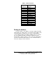
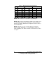
Table 1 - Printer Functions PIOC DB-25 Connector Printer Function 1 2 3 4 5 6 7 8 9 10 11 12 13 14 15 16 17 18 - 25 Strobe Data Bit 1 Data Bit 2 Data Bit 3 Data Bit 4 Data Bit 5 Data Bit 6 Data Bit 7 Data Bit 8 Acknowledge Busy Paper End Select Auto Feed Error Initialize Printer Select Input Ground Setting the Address The base address of the PIOC is set using a eight-position DIP switch, SW1. The eight positions correspond to the I/O address lines of A2 through A9 (see Table 2).
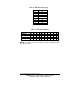
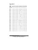
Table 2 - DIP Switch Functions SW1 1 2 3 4 5 6 7 8 I/O Address A9 A8 A7 A6 A5 A4 A3 A2 Table 3 - DIP Switch Weights SW1 Address: Weight: LPT1 (378h): LPT2 (278h): 1 2 3 4 5 6 7 8 X X A9 A8 A7 A6 A5 A4 A3 A2 A1 A0 2 1 8 4 2 1 8 4 2 1 1 1 0 1 1 1 1 0 0 0 1 0 0 1 1 1 1 0 0 0 NOTE: A "1" indicates that the switch is ON and a "0"indicates that the switch is OFF.
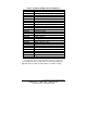
Table 4 - Hardware I/O Map of AT Class Machines Hex Address 000-01F 020-03F 040-05F 060-06F 070-07F 080-09F 0A0-0BF 0C0-0DF 0F0-0FF 1F0-1F8 200-20F 258-25F 278-27F 2E8-2EF 2F8-2FF 300-31F 378-37F 380-38F 3A0-3AF 3B0-3BF 3BC-3BE 3C0-3CF 3D0-3D7 3E8-3EF 3F0-3F7 3F8-3FF Address Function in AT Class Machines DMA controller #1 (8237A-5) interrupt controller #1 (8259A) timer (8254) keyboard (8042) NMI - non maskable interrupt & CMOS RAM DMA page register (74LS612) interrupt controller #2 (8259A) DMA controller #
Using the PIOC as I/O The PIOC may also be used as a general I/O device. The Base Register has eight bi-directional lines. The direction of these lines is based on bit 5 of the Control Register. If bit 5 of the Control Register is a “1”, then the lines of the Base Register are defined as inputs. If bit 5 of the Control Register is a “0”, then these lines are defined as outputs (this is default state after “boot up”).
BIT 0 1 2 3 4 5 6 7 Table 5 - Register Functions and Pinouts Base (378H) Status (379H) Control (37AH) OUTPUT INPUT OUTPUT INPUT OUTPUT INPUT 2 3 4 5 6 7 8 9 2 3 4 5 6 7 8 9 X X X X X X X X X X X 15 13 12 10 11 1 14 16 17 1 14 16 17 See Note 2 See Note2 See Note 3 See Note 3 X X X X NOTE 1: An "X" means no connection to any DB-25 pins. NOTE 2: Bit 4 of the Control Register (37AH) as an output is used to control IRQ7.
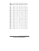
Appendix A SW1: ......... 1 .....2 . ..... 3..... 4 ........5..... 6..... 7........8 .... X.....X Addr.: .....A9 .. A8 . ...A7...A6 ..... A5...A4...A3..... A2 .. A1...A0 Weight:..... 2 .....1 . ..... 8..... 4 ........2..... 1..... 8........4 .... 2..... 1 000 ........... 0 .....0 . ..... 0..... 0 ........0..... 0..... 0........0 .... 0..... 0 004 ........... 0 .....0 . ..... 0..... 0 ........0..... 0..... 0........1 .... 0..... 0 008 ........... 0 .....0 . ..... 0..... 0 ........0..... 0..... 1........0 ...
SW1: ......... 1 .....2 . ..... 3..... 4 ........5..... 6..... 7........8 .... X.....X Addr.: .....A9 .. A8 . ...A7...A6 ..... A5...A4...A3..... A2 .. A1...A0 Weight:..... 2 .....1 . ..... 8..... 4 ........2..... 1..... 8........4 .... 2..... 1 080 ........... 0 .....0 . ..... 1..... 0 ........0..... 0..... 0........0 .... 0..... 0 084 ........... 0 .....0 . ..... 1..... 0 ........0..... 0..... 0........1 .... 0..... 0 088 ........... 0 .....0 . ..... 1..... 0 ........0..... 0..... 1........0 .... 0.....
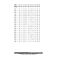
SW1: ......... 1 .....2 . ..... 3..... 4 ........5..... 6..... 7........8 .... X.....X Addr.: .....A9 .. A8 . ...A7...A6 ..... A5...A4...A3..... A2 .. A1...A0 Weight:..... 2 .....1 . ..... 8..... 4 ........2..... 1..... 8........4 .... 2..... 1 100 ........... 0 .....1 . ..... 0..... 0 ........0..... 0..... 0........0 .... 0..... 0 104 ........... 0 .....1 . ..... 0..... 0 ........0..... 0..... 0........1 .... 0..... 0 108 ........... 0 .....1 . ..... 0..... 0 ........0..... 0..... 1........0 .... 0.....
SW1: ......... 1 .....2 . ..... 3..... 4 ........5..... 6..... 7........8 .... X.....X Addr.: .....A9 .. A8 . ...A7...A6 ..... A5...A4...A3..... A2 .. A1...A0 Weight:..... 2 .....1 . ..... 8..... 4 ........2..... 1..... 8........4 .... 2..... 1 180 ........... 0 .....1 . ..... 1..... 0 ........0..... 0..... 0........0 .... 0..... 0 184 ........... 0 .....1 . ..... 1..... 0 ........0..... 0..... 0........1 .... 0..... 0 188 ........... 0 .....1 . ..... 1..... 0 ........0..... 0..... 1........0 .... 0.....
SW1: ......... 1 .....2 . ..... 3..... 4 ........5..... 6..... 7........8 .... X.....X Addr.: .....A9 .. A8 . ...A7...A6 ..... A5...A4...A3..... A2 .. A1...A0 Weight:..... 2 .....1 . ..... 8..... 4 ........2..... 1..... 8........4 .... 2..... 1 200 ........... 1 .....0 . ..... 0..... 0 ........0..... 0..... 0........0 .... 0..... 0 204 ........... 1 .....0 . ..... 0..... 0 ........0..... 0..... 0........1 .... 0..... 0 208 ........... 1 .....0 . ..... 0..... 0 ........0..... 0..... 1........0 .... 0.....
SW1: ......... 1 .....2 . ..... 3..... 4 ........5..... 6..... 7........8 .... X.....X Addr.: .....A9 .. A8 . ...A7...A6 ..... A5...A4...A3..... A2 .. A1...A0 Weight:..... 2 .....1 . ..... 8..... 4 ........2..... 1..... 8........4 .... 2..... 1 280 ........... 1 .....0 . ..... 1..... 0 ........0..... 0..... 0........0 .... 0..... 0 284 ........... 1 .....0 . ..... 1..... 0 ........0..... 0..... 0........1 .... 0..... 0 288 ........... 1 .....0 . ..... 1..... 0 ........0..... 0..... 1........0 .... 0.....
SW1: ......... 1 .....2 . ..... 3..... 4 ........5..... 6..... 7........8 .... X.....X Addr.: .....A9 .. A8 . ...A7...A6 ..... A5...A4...A3..... A2 .. A1...A0 Weight:..... 2 .....1 . ..... 8..... 4 ........2..... 1..... 8........4 .... 2..... 1 300 ........... 1 .....1 . ..... 0..... 0 ........0..... 0..... 0........0 .... 0..... 0 304 ........... 1 .....1 . ..... 0..... 0 ........0..... 0..... 0........1 .... 0..... 0 308 ........... 1 .....1 . ..... 0..... 0 ........0..... 0..... 1........0 .... 0.....
SW1: ......... 1 .....2 . ..... 3..... 4 ........5..... 6..... 7........8 .... X.....X Addr.: .....A9 .. A8 . ...A7...A6 ..... A5...A4...A3..... A2 .. A1...A0 Weight:..... 2 .....1 . ..... 8..... 4 ........2..... 1..... 8........4 .... 2..... 1 380 ........... 1 .....1 . ..... 1..... 0 ........0..... 0..... 0........0 .... 0..... 0 384 ........... 1 .....1 . ..... 1..... 0 ........0..... 0..... 0........1 .... 0..... 0 388 ........... 1 .....1 . ..... 1..... 0 ........0..... 0..... 1........0 .... 0.....
NOTE 1: The addresses marked with an "*" are the addresses normally associated with LPT1 and LPT2. 378 (and sometimes 3BCh) is used as LPT1 and 278h is usually used with LPT2. NOTE 2: The last two bits (A0 and A1), marked with an "X" on SW1, are not used. NOTE 3: A "1" indicates that the switch is ON and a "0" indicates that the switch is OFF.