
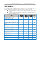
Specifications


SHENZHEN B&T TECHNOLOGY Co., Ltd ZHONGSHAN B&T TECHNOLOGY Co., Ltd
12
6、Design guidance
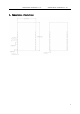
1、Application circuit
2、Recommended Module Package Design Size
Note: This is the BW15 module package diagram, It is recommended to design the
PCB board according to this diagram, so that the module can work normally on the
PCB board; and when designing the pads, please pay attention to the design of
the pads on the PCB. The pad is retracted and offset, and the PCB pad is expanded
from the module pad do not affect the use of the module.
3、Antenna layout requirements
(1)、 the installation position on the motherboard, the following two ways are
recommended:
Scheme 1: put the module on the edge of the motherboard, and the antenna area
extends out of the edge of the motherboard.