
Service manual
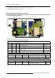
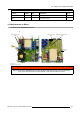


Table Of Contents
- toc
- 1. Safety
- 2. General Info SLM R12+ P
- 3. SLM R12+ P - Parts
- 4. SLM R12+ P - Location of the modules
- 5. SLM R12+ P - Location of the Fans
- 6. Interconnection diagram
- 7. IR Transmitter RC-5 Coded R763569
- 8. Local Keypad & LCD Display
- 9. Communication Module R763768
- 10. Serial Digital Input Module R7632485
- 11. Signal Input Selection R763850 & R763851
- 11.1 General Info
- 11.2 Block Diagram Signal Input Selection 1 & 2
- 11.3 Technical Description Input Selector 1 & 2
- 11.4 Power Supply
- 12. Digital Decoder R763826
- 13. Digital Inputs Backplane R763378
- 14. Power Distribution Backplane R764239
- 15. Lamp Power Supply R7633705
- 15.1 General Info
- 15.2 Technical Info
- 15.3 Interconnection Diagrams
- 15.4 Controls on Board
- 15.5 Technical Description LPS-X In/Out R7632113
- 15.5.1 General
- 15.5.2 Functions on the module:
- 15.5.3 EMC Filter - Rush-in Current Limit - Mains Rectifier.
- 15.5.4 On-board SMPS.
- 15.5.5 Secondary circuit of the LPS.
- 15.5.6 Measurement of the lamp voltage.
- 15.5.7 Lamp Current Measurement.
- 15.5.8 Boost up circuit.
- 15.5.9 Fan drive
- 15.5.10 LAMP_ON green LED indication.
- 15.6 Technical Description LPS-X Processing R7632105
- 15.7 Pin Assignment Connectors on Board
- 15.8 Adjustments on Board
- 16. Start Pulse Generator (SPG) R763512
- 17. Switch Mode Power Supply (SMPS) R764349
- 18. Temperature & Motor Control Module R764203
- 19. Formatter Interface Board (FIB) R764346
- 20. CPU Module R7638858
- 21. Pixel Map Processor Module R764115
- 22. Infra Red Receiver Module R763261
- 23. Ambient Temperature Sensor R762790
- 24. Projector Tilt Switch R764240
- 25. Light Output Sensor R763294
- 26. Lamp Info Module R763295
- 27. Maintenance
- 27.1 Lens Block
- 27.2 Cleaning/Replacement of the Dust Filters
- 27.3 Lamp Replacement
- 27.4 Re-convergence
- 27.4.1 Re-Convergence Kit
- 27.4.2 Preparation Projector for Re-Convergence
- 27.4.3 Re-convergence the Light Engine
- 27.5 Engine Replacement
- 27.5.1 Safety Instructions
- 27.5.2 Access to Image Processor Unit
- 27.5.3 Removing the Engine
- 27.5.3.1 Overview connections behind input box
- 27.5.3.2 Disconnecting the formatter and DMD connections
- 27.5.3.3 Removing the disconnected cables
- 27.5.3.4 Disconnect the lens sensor cable
- 27.5.3.5 Disconnect the shutter
- 27.5.3.6 Disconnect the lens holder ground leads
- 27.5.3.7 Disconnecting the engine fans
- 27.5.3.8 Removing the engine
- 27.5.4 Installing a new engine
- 27.5.5 Re-assembling the projector
- 27.6 Replacement of the Light Integration Rod
- 28. Upgrade with Air Filters
- 28.1 Air Filter Upgrade Kit for SLM R12+
- 28.2 Disassembling the projector for Cover replacement
- 28.3 Reassembling the projector with kit parts
- 28.3.1 Step by step actions
- 28.3.2 Reassembling Steps
- 28.3.2.1 Adaptation of the Safety cable tightening unit
- 28.3.2.2 Mounting the Bottom Cover with Air Filters
- 28.3.2.3 Mounting the Carrying handle fixation studs
- 28.3.2.4 Mounting the Carrying Handle
- 28.3.2.5 Mounting the removed Stacking interlocks
- 28.3.2.6 Mounting the IR Receiver Unit
- 28.3.2.7 Mounting the Bottom Cover with Air Filters
- 29. Overview of the Electrical Diagrams
- A. Specifications
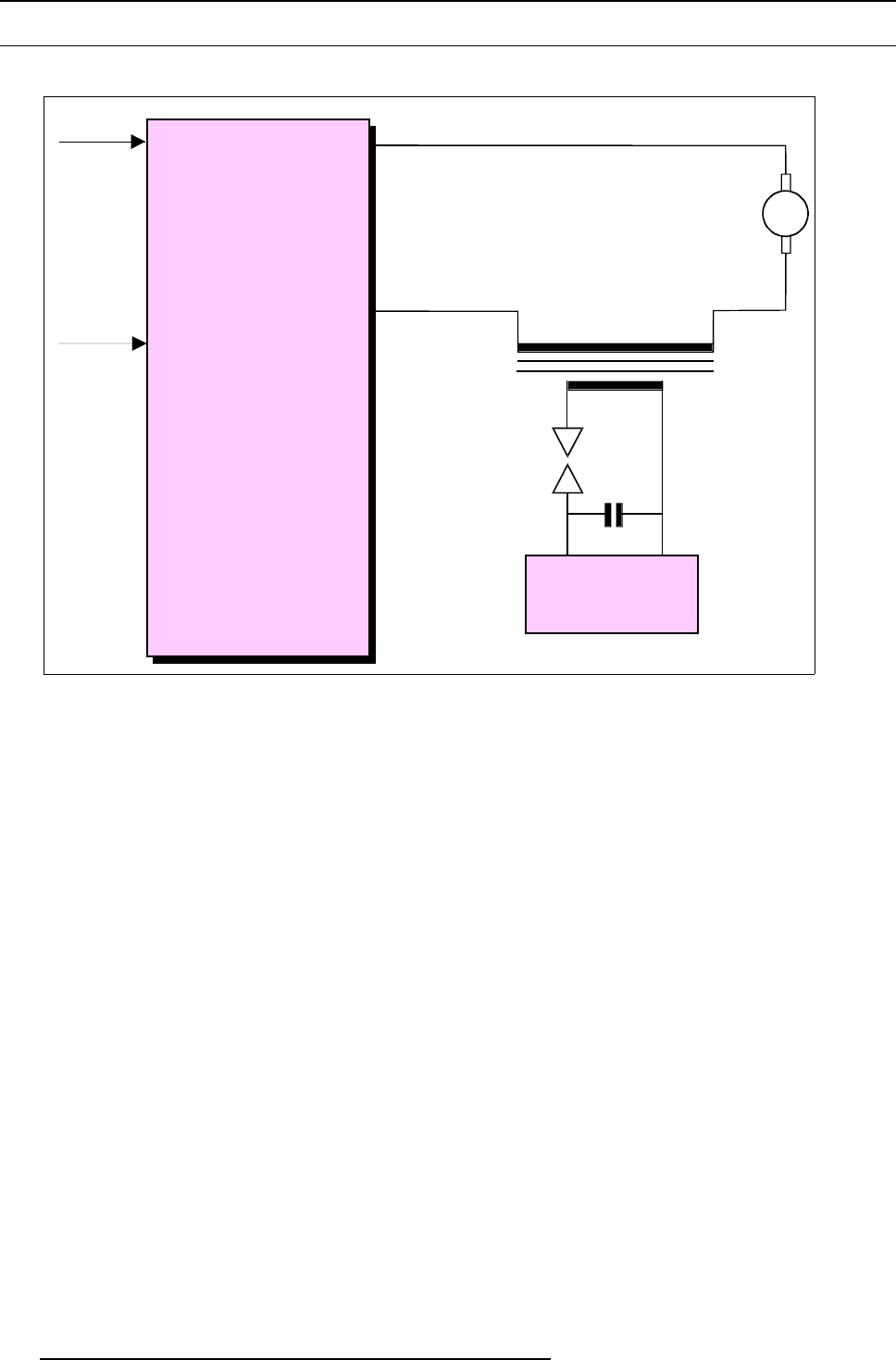
16. Start Pulse Generator (SPG) R763512
16.2 Technical Info
Block Diagram
Max. 100Vdc output voltage
Secondary side
Lamp Power Supply
230VAC
mains
C
+
-
Xenon Arc Lamp
2.2kW
Superimposing
transformer
Spark gap
Capacitor loading circuit
(active during lamp startup)
Block diagram Start Pulse Generator
Image 16-2
Block diagram SPG
Technical Description
The transformer is triggered at the primary by a periodical discharge of a few high voltage capacitors (C5, C6, C7) through two spark
gaps (SA1, SA2). This generates an energy pulse of a few megahertz. The voltage at the secondary is several times higher than
the voltage on the primary.
The high voltage capacitors itself are charged by a Switched Mode Power Supply. All active components of the SMPS are on the
subunit of the SPG.
At the beginning of a switching cycle the Mosfet Q1 it turned on. The current through Q1 and the primary of T1 ramps up, putting
energy into T1. The HV diodes on the secondary are at that time off. The current is measured by resistors R5 and R6. When it
reaches about 5 A the control IC I1 switches Q1 off. The energy stored in T1 is now charging C5, C6 and C7 via a current through
D3.
The capacitor C4 and the diode D2 form a clamping circuit for the high voltage peaks on the secondary of T1. The capacitor C4 is
charged through D2 at the beginning of the on period of Q1. To limit the peak current at that time, L1 is added. Because L1 would
generate a high voltage when Q1
is switched off, a snubber network formed around D1, R1 and C3 is also added.
The IC1 is a low power current mode PWM IC (Pulse Width Modulation). It is activated when the lamp voltage reaches about 85V.
This is the minimum dc lamp voltage for igniting the lamp. The moment the lamp voltage drops below this voltage, it means the lamp
is ignited and the IC is disactivated.
Detection of the lamp volta
ge is done by Q2 and Z1. When the voltage across R10 becomes higher than the zener voltage, Q2
begins to conduct and delivers power to IC1.
A turn-on delay of about one second is added by the network C4, R2 and D1 to make sure the dc lamp voltage is stabilized.
The switching frequency is determined by R1 and C5 and is set at about 12.5kHz. D2 and D3 protect the circuit against reversed
polarity.
126
R5976820 SLM R12+ PERFORMER 08/03/2005