
Data Sheet


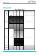
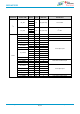
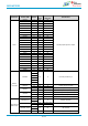
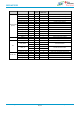
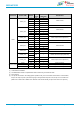
Table Of Contents
- General Description
- Key Features
- Applications
- Device Family
- Contents
- 1. References
- 2. Block Diagram
- 3. Terminal Configuration and Functions
- 4. Specifications
- 5. Detailed Description
- 6. Applications, Implementation, and Layout
- 7. Mechanical Specifications
- 8. Ordering Information
- 9. Revision History
- 10. Regulatory

info@bdecomm.com
BDE Technology Inc.
BDE-WF3235
BDE Dual-Band WiFi MCU Module
Datasheet
Datasheet
30 / 77
3.4 Drive Strength and Reset States for Analog-Digital Multiplexed Pins
Table 3-4 describes the use, drive strength, and default state of analog- and digital-multiplexed pins at first-
time power up and reset (nRESET pulled low).
Table 3-4. Drive Strength and Reset States for Analog-Digital Multiplexed Pins
PIN
BOARD LEVEL
CONFIGURATION AND USE
DEFAULT STATE AT FIRST POWER
UP OR FORCED RESET
STATE AFTER
CONFIGURATION OF
ANALOG SWITCHES
(ACTIVE, LPDS, and HIB
POWER MODES)
MAXIMUM
EFFECTIVE
DRIVE
STRENGTH
(mA)
42
Generic I/O
Analog is isolated. The digital I/O cell is
also isolated.
Determined by the I/O state, as
are other digital I/Os.
4
44
Generic I/O
Analog is isolated. The digital I/O cell is
also isolated.
Determined by the I/O state, as
are other digital I/Os.
4
47
Analog signal
(1.8-V absolute, 1.46-V full scale)
ADC is isolated. The digital I/O cell is
also isolated.
Determined by the I/O state, as
are other digital I/Os.
4
48
Analog signal
(1.8-V absolute, 1.46-V full scale)
ADC is isolated. The digital I/O cell is
also isolated.
Determined by the I/O state, as
are other digital I/Os.
4
49
Analog signal
(1.8-V absolute, 1.46-V full scale)
ADC is isolated. The digital I/O cell is
also isolated.
Determined by the I/O state, as
are other digital I/Os.
4
50
Analog signal
(1.8-V absolute, 1.46-V full scale)
ADC is isolated. The digital I/O cell is
also isolated.
Determined by the I/O state, as
are other digital I/Os.
4
3.5 Pad State After Application of Power to Chip, but Before Reset Release
When a stable power is applied to the BDE-WF3235 module for the first time or when supply voltage is restored
to the proper value following a prior period with supply voltage below 1.5V, the level of the digital pads are
undefined in the period starting from the release of nRESET and until the DIG_DCDC of the
CC3235S/CC3235SF chip powers up. This period is less than approximately 10ms. During this period, pads
can be internally pulled weakly in either direction. If a certain set of pins are required to have a definite value
during this pre-reset period, an appropriate pullup or pulldown must be used at the board level. The
recommended value of these external pullup or pulldown resistors is 2.7kΩ.