
Data Sheet
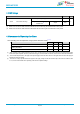
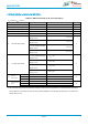
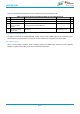
Table Of Contents
- General Description
- Key Features
- Applications
- Device Family
- Contents
- 1. References
- 2. Block Diagram
- 3. Terminal Configuration and Functions
- 4. Specifications
- 5. Detailed Description
- 6. Applications, Implementation, and Layout
- 7. Mechanical Specifications
- 8. Ordering Information
- 9. Revision History
- 10. Regulatory

info@bdecomm.com
BDE Technology Inc.
BDE-WF3235
BDE Dual-Band WiFi MCU Module
Datasheet
Datasheet
31 / 77
3.6 Connections for Unused Pins
All unused pin should be configured as stated in Table 3-5.
Table 3-5. Connections for Unused Pins
FUNCTION
SIGNAL DESCRIPTION
PIN NUMBER
ACCEPTABLE PRACTICE
GPIO
General-purpose input or output
Wake up I/O source should not be floating during hibernate.
All the I/O pins will float while in Hibernate and Reset
states. Ensure pullup and pulldown resistors are available
on board to maintain the state of the I/O.
Leave unused GPIOs as NC
No Connect
NC
20, 31, 33, 39,
41, 45
Unused pin, leave as NC.
SOP
Configuration sense-on-power
23, 24, 34
Leave as NC (Modules contain internal 100-kΩ pulldown
resistors on the SOP lines). An external 10-kΩ pullup resistor
is required to pull these pins high. See Section 5.11 for
SOP[2:0] configuration modes.
Reset
RESET input for the device
Never leave the reset pin floating
JTAG
JTAG interface
Leave as NC if unused