
Data Sheet
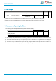
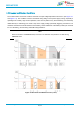
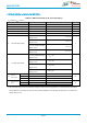
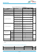
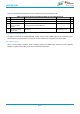
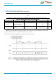
Table Of Contents
- General Description
- Key Features
- Applications
- Device Family
- Contents
- 1. References
- 2. Block Diagram
- 3. Terminal Configuration and Functions
- 4. Specifications
- 5. Detailed Description
- 6. Applications, Implementation, and Layout
- 7. Mechanical Specifications
- 8. Ordering Information
- 9. Revision History
- 10. Regulatory

info@bdecomm.com
BDE Technology Inc.
BDE-WF3235
BDE Dual-Band WiFi MCU Module
Datasheet
Datasheet
33 / 77
4.2 ESD Ratings
VALUE
UNIT
V
ESD
Electrostatic discharge
Human body model (HBM), per ANSI/ESDA/JEDEC JS001
(1)
±2000
V
Charged device model (CDM), per
JESD22-C101
(2)
All pins
±500
(1) JEDEC document JEP155 states that 500-V HBM allows safe manufacturing with a standard ESD control process.
(2) JEDEC document JEP157 states that 250-V CDM allows safe manufacturing with a standard ESD control process.
4.3 Recommended Operating Conditions
Over operating free-air temperature range (unless otherwise noted)
(2) (1)
(3)
PARAMETER
MIN
TYP
MAX
UNIT
V
BAT
2.3
3.3
3.6
V
Operating temperature
–40
25
85
°C
Ambient thermal slew
–20
20
°C/minute
(1) When operating at an ambient temperature of over 75°C, the transmit duty cycle must remain below 50% to avoid the auto-protect
feature of the power amplifier. If the auto-protect feature triggers, the device takes a maximum of 60 seconds to restart the transmission.
(2) To ensure WLAN performance, the ripple on the power supply must be less than ±300 mV. The ripple should not cause the supply to
fall below the brownout voltage.
(3) The minimum voltage specified includes the ripple on the supply voltage and all other transient dips. The brownout condition is also
2.1 V, and care must be taken when operating at the minimum specified voltage.