
Data Sheet
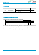
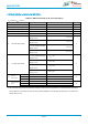
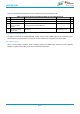
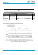
Table Of Contents
- General Description
- Key Features
- Applications
- Device Family
- Contents
- 1. References
- 2. Block Diagram
- 3. Terminal Configuration and Functions
- 4. Specifications
- 5. Detailed Description
- 6. Applications, Implementation, and Layout
- 7. Mechanical Specifications
- 8. Ordering Information
- 9. Revision History
- 10. Regulatory

info@bdecomm.com
BDE Technology Inc.
BDE-WF3235
BDE Dual-Band WiFi MCU Module
Datasheet
Datasheet
36 / 77
4.5 Electrical Characteristics for GPIO Pins
Table 4-3. GPIO Pins Except 25, 26, 42, and 44 (25°C)
(1)
T
A
= 25°C, V
BAT
= 3.3 V
PARAMETER
TEST CONDITIONS
MIN NOM MAX
UNIT
C
IN
Pin capacitance
4
pF
V
IH
High-level input voltage
0.65 × V
DD
V
DD
+ 0.5 V
V
V
IL
Low-level input voltage
–0.5 0.35 × V
DD
V
I
IH
High-level input current
5
nA
I
IL
Low-level input current
5
nA
V
OH
High-level output voltage
IL = 2 mA; configured I/O drive
strength = 2 mA;
2.4 V ≤ V
DD
< 3.6 V
V
DD
× 0.8
V
IL = 4 mA; configured I/O drive
strength = 4 mA;
2.4 V ≤ V
DD
< 3.6 V
V
DD
× 0.7
IL = 6 mA; configured I/O drive
strength = 6 mA;
2.4 V ≤ V
DD
< 3.6 V
V
DD
× 0.7
IL = 2 mA; configured I/O drive
strength = 2 mA;
2.3 V ≤ V
DD
< 2.4 V
V
DD
× 0.75
V
OL
Low-level output voltage
IL = 2 mA; configured I/O drive
strength = 2 mA;
2.4 V ≤ V
DD
< 3.6 V
V
DD
× 0.2
V
IL = 4 mA; configured I/O drive
strength = 4 mA;
2.4 V ≤ V
DD
< 3.6 V
V
DD
× 0.2
IL = 6 mA; configured I/O drive
strength = 6 mA;
2.4 V ≤ V
DD
< 3.6 V
V
DD
× 0.2
IL = 2 mA; configured I/O drive
strength = 2 mA;
2.3 V ≤ V
DD
< 2.4 V
V
DD
× 0.25
IOH
High-level
source current
2-mA drive
2
mA
4-mA drive
4
6-mA drive
6
IOL
Low-level sink
current
2-mA drive
2
mA
4-mA drive
4
6-mA drive
6
(1) We recommend using the lowest possible drive strength that is adequate for the applications. This recommendation minimizes the
risk of interference to the WLAN radio and reduces any potential degradation of RF sensitivity and performance. The default drive
strength setting is 6 mA.