
Data Sheet
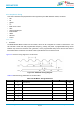

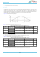
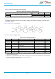
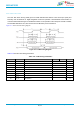
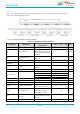

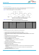
Table Of Contents
- General Description
- Key Features
- Applications
- Device Family
- Contents
- 1. References
- 2. Block Diagram
- 3. Terminal Configuration and Functions
- 4. Specifications
- 5. Detailed Description
- 6. Applications, Implementation, and Layout
- 7. Mechanical Specifications
- 8. Ordering Information
- 9. Revision History
- 10. Regulatory

info@bdecomm.com
BDE Technology Inc.
BDE-WF3235
BDE Dual-Band WiFi MCU Module
Datasheet
Datasheet
41 / 77
4.8.5 Peripherals Timing
This section describes the peripherals that are supported by the BDE-WF3235 module, as follows:
• SPI
• I
2
S
• GPIOs
• I
2
C
• IEEE 1149.1 JTAG
• ADC
• Camera parallel port
• External flash
• UART
• SD Host
• Timers
4.8.5.1 SPI
SPI Master
The BDE-WF3235 MCU includes one SPI module, which can be configured as a master or slave device. The
SPI includes a serial clock with programmable frequency, polarity, and phase; a programmable timing control
between chip select and external clock generation; and a programmable delay before the first SPI word is
transmitted. Slave mode does not include a dead cycle between two successive words.
Figure 4-5 shows the timing diagram for the SPI master.
Figure 4-5. SPI Master Timing Diagram
Table 4-8 lists the timing parameters for the SPI master.
Table 4-8. SPI Master Timing Parameters
ITEM
NAME
DESCRIPTION
MIN
MAX
UNIT
F
(1)
Clock frequency
20
MHz
T2
T
clk
(1)
Clock period
50
ns
D
(1)
Duty cycle
45% 55%
T6
t
IS
(1)
RX data setup time
1
ns
T7
t
IH
(1)
RX data hold time
2
ns
T8
t
OD
(1)
TX data output delay
8.5
ns
T9
t
OH
(1)
TX data hold time
8
ns
(1) Timing parameter assumes a maximum load of 20 pF.