
Data Sheet
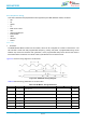

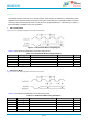
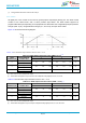
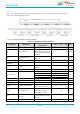
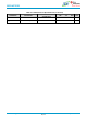
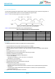
Table Of Contents
- General Description
- Key Features
- Applications
- Device Family
- Contents
- 1. References
- 2. Block Diagram
- 3. Terminal Configuration and Functions
- 4. Specifications
- 5. Detailed Description
- 6. Applications, Implementation, and Layout
- 7. Mechanical Specifications
- 8. Ordering Information
- 9. Revision History
- 10. Regulatory

info@bdecomm.com
BDE Technology Inc.
BDE-WF3235
BDE Dual-Band WiFi MCU Module
Datasheet
Datasheet
45 / 77
Table 4-14 lists the input transition time parameters.
Table 4-14. GPIO Input Transition Time Parameters
MIN
MAX
UNIT
t
r
Input transition time (t
r
, t
f
), 10% to 90%
1
3
ns
t
f
1
3
ns
4.8.5.4 I
2
C
The BDE-WF3235 MCU includes one I
2
C module operating with standard (100 kbps) or fast (400 kbps)
transmission speeds.
Figure 4-10 shows the I
2
C timing diagram.
Figure 4-10. I
2
C Timing Diagram
Table 4-15 lists the I
2
C timing parameters.
Table 4-15. I
2
C Timing Parameters
(3)
ITEM
NAME
DESCRIPTION
MIN MAX
UNIT
T2
t
LP
Clock low period
See
(1)
System clock
T3
t
SRT
SCL/SDA rise time
See
(2)
ns
T4
t
DH
Data hold time
NA
T5
t
SFT
SCL/SDA fall time
3
ns
T6
t
HT
Clock high time
See
(1)
System clock
T7
t
DS
Data setup time
tLP/2
System clock
T8
t
SCSR
Start condition setup time
36
System clock
T9
t
SCS
Stop condition setup time
24
System clock
(1) This value depends on the value programmed in the clock period register of I
2
C. Maximum output frequency is the result of the minimal
value programmed in this register.
(2) Because I
2
C is an open-drain interface, the controller can drive logic 0 only. Logic is the result of external pullup. Rise time depends
on the value of the external signal capacitance and external pullup register.
(3) All timing is with 6-mA drive and 20-pF load.