
Datasheet


ST72334J/N, ST72314J/N, ST72124J
112/153
FUNCTIONAL OPERATING CONDITIONS (Cont’d)
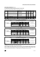
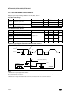
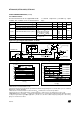
Figure 60. High LVD Threshold Versus V
DD
and f
OSC
for ROM devices
2)
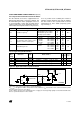
Figure 61. Medium LVD Threshold Versus V
DD
and f
OSC
for ROM devices
2)
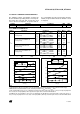
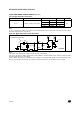
Figure 62. Low LVD Threshold Versus V
DD
and f
OSC
for ROM devices
2)3)
Notes:
1. LVD typical data are based on T
A
=25°C. They are given only as design guidelines and are not tested.
2. The minimum V
DD
rise time rate is needed to insure a correct device power-on and LVD reset. Not tested in production.
3. If the low LVD threshold is selected, when V
DD
falls below 3.2V, (V
DD
minimum operating voltage), the device is guar-
anteed to continue functioning until it goes into reset state. The specified V
DD
min. value is necessary in the device power
on phase, but during a power down phase or voltage drop the device will function below this min. level.
f
OSC
[MHz]
SUPPLY VOLTAGE [V]
16
8
0
2.5 3 3.5 4 4.5 5 5.5
FUNCTIONAL AREA
DEVICE UNDER
RESET
IN THIS AREA
FUNCTIONALITY
NOT GUARANTEED
IN THIS AREA
V
IT-
≥3.85
f
OSC
[MHz]
SUPPLY VOLTAGE [V]
16
8
0
2.5 3 V
IT-
≥3.5V 4 4.5 5 5.5
FUNCTIONAL AREA
DEVICE UNDER
RESET
IN THIS AREA
FUNCTIONALITY
NOT GUARANTEED
IN THIS AREA
f
OSC
[MHz]
SUPPLY VOLTAGE [V]
16
8
0
2.5 V
IT-
≥3.00V 3.5 4 4.5 5 5.5
FUNCTIONAL AREA
DEVICE UNDER
RESET
IN THIS AREA
FUNCTIONALITY
NOT GUARANTEED
IN THIS AREA