
Datasheet


ST72334J/N, ST72314J/N, ST72124J
129/153
I/O PORT PIN CHARACTERISTICS (Cont’d)
16.8.2 Output Driving Current
Subject to general operating conditions for V
DD
, f
OSC
, and T
A
unless otherwise specified.
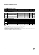
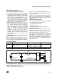
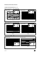
Figure 84. Typical V
OL
at V
DD
=5V (standard)
Figure 85. Typical V
OL
at V
DD
=5V (high-sink)
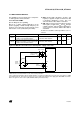
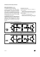
Figure 86. Typical V
OH
at V
DD
=5V
Notes:
1. The I
IO
current sunk must always respect the absolute maximum rating specified in Section 16.2.2 and the sum of I
IO
(I/O ports and control pins) must not exceed I
VSS
.
2. The I
IO
current sourced must always respect the absolute maximum rating specified in Section 16.2.2 and the sum of
I
IO
(I/O ports and control pins) must not exceed I
VDD
. True open drain I/O pins does not have V
OH
.
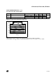
Symbol Parameter Conditions Min Max Unit
V
OL
1)
Output low level voltage for a standard I/O pin
when 8 pins are sunk at same time
(see Figure 84 and Figure 87)
V
DD
=5V
I
IO
=+5mA T
A
≤85°C
T
A
≥85°C
1.3
1.5
V
I
IO
=+2mA T
A
≤85°C
T
A
≥85°C
0.65
0.75
Output low level voltage for a high sink I/O pin
when 4 pins are sunk at same time
(see Figure 85 and Figure 88)
I
IO
=+20mA,T
A
≤85°C
T
A
≥85°C
1.5
1.7
I
IO
=+8mA T
A
≤85°C
T
A
≥85°C
0.75
0.85
V
OH
2)
Output high level voltage for an I/O pin
when 4 pins are sourced at same time
(see Figure 86 and Figure 89)
I
IO
=-5mA, T
A
≤85°C
T
A
≥85°C
V
DD
-1.6
V
DD
-1.7
I
IO
=-2mA T
A
≤85°C
T
A
≥85°C
V
DD
-0.8
V
DD
-1.0
0246810
Iio [mA]
0
0.5
1
1.5
2
2.5
Vol [V] at Vdd=5V
Ta=-40°C
Ta=25°C
Ta=85°C
Ta=125°C
0 5 10 15 20 25 30
Iio [mA]
0
0.5
1
1.5
2
Vol [V] at Vdd=5V
Ta=-40°C
Ta=25°C
Ta=85°C
Ta=125°C
-8 -6 -4 -2 0
Iio [mA]
1
2
3
4
5
6
Voh [V] at Vdd=5V
Ta=-40°C
Ta=25°C
Ta=85°C
Ta=125°C