
Datasheet


ST72334J/N, ST72314J/N, ST72124J
131/153
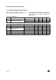
16.9 CONTROL PIN CHARACTERISTICS
16.9.1 Asynchronous RESET
Pin
Subject to general operating conditions for V
DD
, f
OSC
, and T
A
unless otherwise specified.
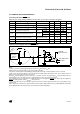
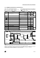
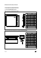
Figure 90. Typical Application with RESET
pin
8)
Notes:
1. Unless otherwise specified, typical data are based on T
A
=25°C and V
DD
=5V.
2. Data based on characterization results, not tested in production.
3. Hysteresis voltage between Schmitt trigger switching levels. Based on characterization results, not tested.
4. The I
IO
current sunk must always respect the absolute maximum rating specified in Section 16.2.2 and the sum of I
IO
(I/O ports and control pins) must not exceed I
VSS
.
5. The R
ON
pull-up equivalent resistor is based on a resistive transistor (corresponding I
ON
current characteristics de-
scribed in Figure 91). This data is based on characterization results, not tested in production.
6. To guarantee the reset of the device, a minimum pulse has to be applied to RESET
pin. All short pulses applied on
RESET pin with a duration below t
h(RSTL)in
can be ignored.
7. The reset network (the resistor and two capacitors) protects the device against parasitic resets, especially in a noisy
environments.
8. The output of the external reset circuit must have an open-drain output to drive the ST7 reset pad. Otherwise the device
can be damaged when the ST7 generates an internal reset (LVD or watchdog).
Symbol Parameter Conditions Min Typ
1)
Max Unit
V
IL
Input low level voltage
2)
0.3xV
DD
V
V
IH
Input high level voltage
2)
0.7xV
DD
V
hys
Schmitt trigger voltage hysteresis
3)
400 mV
V
OL
Output low level voltage
4)
(see Figure 92, Figure 93)
V
DD
=5V
I
IO
=+5mA 0.68 0.95
V
I
IO
=+2mA 0.28 0.45
R
ON
Weak pull-up equivalent resistor
5)
V
IN
=V
SS
V
DD
=5V 20 40 60
kΩ
V
DD
=3.4V 80 100 120
t
w(RSTL)out
Generated reset pulse duration
External pin or
internal reset sources
6
30
1/f
SFOSC
µs
t
h(RSTL)in
External reset pulse hold time
6)
20 µs
t
g(RSTL)in
Filtered glitch duration
7)
100 ns
RESET
V
DD
WATCHDOG RESET
ST72XXX
LVD RESET
INTERNAL
R
ON
0.1µF
V
DD
0.1µF
V
DD
4.7kΩ
EXTERNAL
RESET
CIRCUIT
8)
RESET CONTROL
OPTION
AL
USER