
Datasheet


ST72334J/N, ST72314J/N, ST72124J
138/153
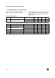
16.12 8-BIT ADC CHARACTERISTICS
Subject to general operating conditions for V
DD
, f
OSC
, and T
A
unless otherwise specified.
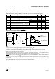
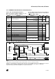
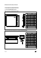
Figure 98. Typical Application with ADC
Notes:
1. Unless otherwise specified, typical data are based on T
A
=25°C and V
DD
-V
SS
=5V. They are given only as design guide-
lines and are not tested.
2. When V
DDA
and V
SSA
pins are not available on the pinout, the ADC refer to V
DD
and V
SS
.
3. Any added external serial resistor will downgrade the ADC accuracy (especially for resistance greater than 10kΩ). Data
based on characterization results, not tested in production.
4. The stabilization time of the AD converter is masked by the first t
LOAD
. The first conversion after the enable is then
always valid.
Symbol Parameter Conditions Min Typ
1)
Max Unit
f
ADC
ADC clock frequency 4 MHz
V
AIN
Conversion range voltage
2)
V
SSA
V
DDA
V
R
AIN
External input resistor 10
3)
kΩ
C
ADC
Internal sample and hold capacitor 6 pF
t
STAB
Stabilization time after ADC enable
f
CPU
=8MHz, f
ADC
=4MHz
0
4)
µs
t
ADC
Conversion time (Sample+Hold) 3
- Sample capacitor loading time
- Hold conversion time
4
8
1/f
ADC
AINx
ST72XXX
C
IO
~2pF
V
DD
I
L
±1µA
V
T
0.6V
V
T
0.6V
V
AIN
R
AIN
V
DDA
V
SSA
0.1µF
V
DD
ADC