
Datasheet


ST72334J/N, ST72314J/N, ST72124J
32/153
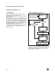
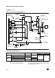
9.5 SUPPLY, RESET AND CLOCK REGISTER DESCRIPTION
Read/Write
Reset Value: 000x 000x (xxh)
Bit 7:5 = Reserved, always read as 0.
Bit 4 = LVDRF
LVD reset flag
This bit indicates that the last RESET was gener-
ated by the LVD block. It is set by hardware (LVD
reset) and cleared by software (writing zero). See
WDGRF flag description for more details. When
the LVD is disabled by option byte, the LVDRF bit
value is undefined.
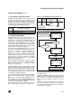
Bit 3 = Reserved, always read as 0.
Bit 2 = CSSIE
Clock security syst
.
interrupt enable
This bit enables the interrupt when a disturbance
is detected by the clock security system (CSSD bit
set). It is set and cleared by software.
0: Clock security system interrupt disabled
1: Clock security system interrupt enabled
Refer to Table 5, “Interrupt mapping,” on page 34
for more details on the CSS interrupt vector. When
the CSS is disabled by option byte, the CSSIE bit
has no effect.
Bit 1 = CSSD
Clock security system detection
This bit indicates that the safe oscillator of the
clock security system block has been selected by
hardware due to a disturbance on the main clock
signal (f
OSC
). It is set by hardware and cleared by
reading the CRSR register when the original oscil-
lator recovers.
0: Safe oscillator is not active
1: Safe oscillator has been activated
When the CSS is disabled by option byte, the
CSSD bit value is forced to 0.
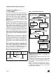
Bit 0 = WDGRF
Watchdog reset flag
This bit indicates that the last RESET was gener-
ated by the watchdog peripheral. It is set by hard-
ware (Watchdog RESET) and cleared by software
(writing zero) or an LVD RESET (to ensure a sta-
ble cleared state of the WDGRF flag when the
CPU starts).
Combined with the LVDRF flag information, the
flag description is given by the following table.
Application notes
The LVDRF flag is not cleared when another RE-
SET type occurs (external or watchdog), the
LVDRF flag remains set to keep trace of the origi-
nal failure.
In this case, a watchdog reset can be detected by
software while an external reset can not.
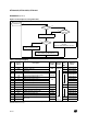
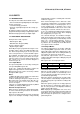
Table 4. Clock, Reset and Supply Register Map and Reset Values
70
000
LVD
RF
0
CSS
IE
CSS
D
WDG
RF
RESET Sources LVDRF WDGRF
External RESET pin 0 0
Watchdog 0 1
LVD 1 X
Address
(Hex.)
Register
Label
76543210
002Bh
CRSR
Reset Value 0 0 0
LVDRF
x0
CFIE
0
CSSD
0
WDGRF
x