
Specifications


ST72104Gx, ST72215Gx, ST72216Gx, ST72254Gx
105/141
13.5 CLOCK AND TIMING CHARACTERISTICS
Subject to general operating conditions for V
DD
, f
OSC
, and T
A
.
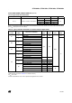
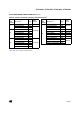
13.5.1 General Timings
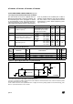
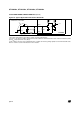
13.5.2 External Clock Source
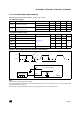
Figure 63. Typical Application with an External Clock Source
Notes:
1. Data based on typical application software.
2. Time measured between interrupt event and interrupt vector fetch. ∆t
c(INST)
is the number of t
CPU
cycles needed to finish
the current instruction execution.
3. Data based on design simulation and/or technology characteristics, not tested in production.
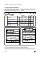
Symbol Parameter Conditions Min Typ
1)
Max Unit
t
c(INST)
Instruction cycle time
2 3 12 t
CPU
f
CPU
=8MHz 250 375 1500 ns
t
v(IT)
Interrupt reaction time
2)
t
v(IT)
= ∆t
c(INST)
+ 10
10 22 t
CPU
f
CPU
=8MHz 1.25 2.75 µs
Symbol Parameter Conditions Min Typ Max Unit
V
OSC1H
OSC1 input pin high level voltage
see Figure 63
0.7xV
DD
V
DD
V
V
OSC1L
OSC1 input pin low level voltage V
SS
0.3xV
DD
t
w(OSC1H)
t
w(OSC1L)
OSC1 high or low time
3)
15
ns
t
r(OSC1)
t
f(OSC1)
OSC1 rise or fall time
3)
15
I
L
OSCx Input leakage current V
SS
≤V
IN
≤V
DD
±1 µA
OSC1
OSC2
f
OSC
EXTERNAL
ST72XXX
CLOCK SOURCE
Not connected internally
V
OSC1L
V
OSC1H
t
r(OSC1)
t
f(OSC1)
t
w(OSC1H)
t
w(OSC1L)
I
L
90%
10%