
Specifications


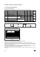


ST72104Gx, ST72215Gx, ST72216Gx, ST72254Gx
116/141
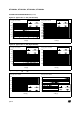
EMC CHARACTERISTICS (Cont’d)
13.7.3 ESD Pin Protection Strategy
To protect an integrated circuit against Electro-
Static Discharge the stress must be controlled to
prevent degradation or destruction of the circuit el
-
ements. The stress generally affects the circuit el-
ements which are connected to the pads but can
also affect the internal devices when the supply
pads receive the stress. The elements to be pro
-
tected must not receive excessive current, voltage
or heating within their structure.
An ESD network combines the different input and
output ESD protections. This network works, by al
-
lowing safe discharge paths for the pins subjected
to ESD stress. Two critical ESD stress cases are
presented in
Figure 73 and Figure 74 for standard
pins and in Figure 75 and Figure 76 for true open
drain pins.
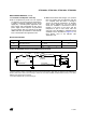
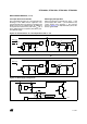
Standard Pin Protection
To protect the output structure the following ele-
ments are added:
– A diode to V
DD
(3a) and a diode from V
SS
(3b)
– A protection device between V
DD
and V
SS
(4)
To protect the input structure the following ele-
ments are added:
– A resistor in series with the pad (1)
– A diode to V
DD
(2a) and a diode from V
SS
(2b)
– A protection device between V
DD
and V
SS
(4)
Figure 73. Positive Stress on a Standard Pad vs. V
SS
Figure 74. Negative Stress on a Standard Pad vs. V
DD
IN
V
DD
V
SS
(1)
(2a)
(2b)
(4)
OUT
V
DD
V
SS
(3a)
(3b)
Main path
Path to avoid
IN
V
DD
V
SS
(1)
(2a)
(2b)
(4)
OUT
V
DD
V
SS
(3a)
(3b)
Main path